Package and semiconductor device

A semiconductor and device technology, which is applied in the field of semiconductor devices, can solve the problems of increasing the number of steps, and achieve the effects of suppressing temperature rise, improving fixing strength, and suppressing unevenness

Inactive Publication Date: 2009-02-11
PANASONIC INDAL DEVICES SUNX
View PDF1 Cites 3 Cited by
  • Summary
  • Abstract
  • Description
  • Claims
  • Application Information

AI Technical Summary

Problems solved by technology

However, it is necessary to form a connection portion having terminals for connecting wires to the respective packages, which creates a problem that the number of steps employed in the manufacturing process significantly increases

Method used


Image

  • Package and semiconductor device
  • Package and semiconductor device
  • Package and semiconductor device

Examples


no. 1 example

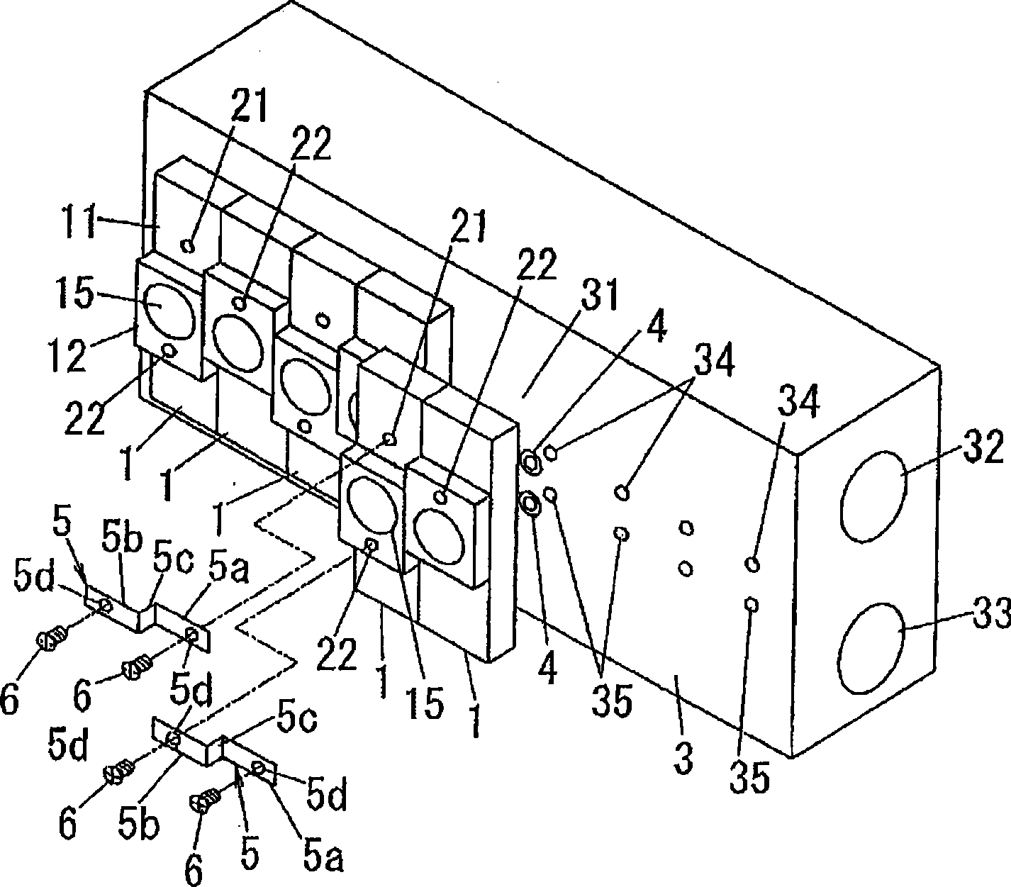
[0052] The package to be described below is, for example, explained by employing a case where the package accommodates a UV-ray light emitting diode as a semiconductor element. Incidentally, in the present invention, not only UV-ray light-emitting diodes that emit light in the ultraviolet wavelength range are used, but light-emitting diodes other than UV-ray light-emitting diodes, such as light-emitting diodes that emit light in the visible wavelength range, can also be used to constitute the package. diode.

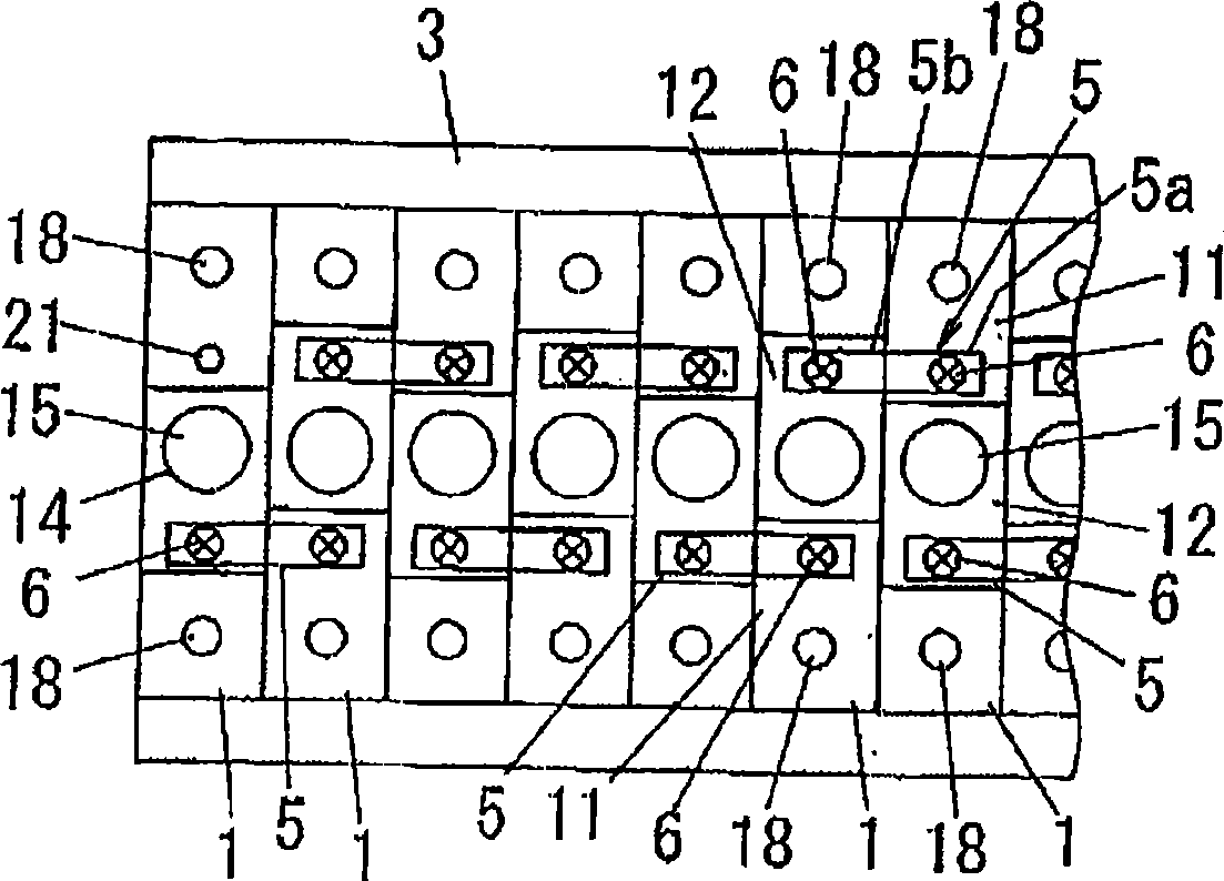
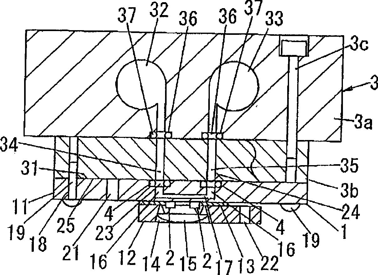
[0053] Such as Figures 3 to 5C As shown, the package 1 is constructed as a layered product produced by laminating a base substrate 11 made of a metal plate on which UV-ray light emitting diodes 2 are mounted, a cover substrate 12 and an insulating material layer 13, The cover substrate 12 is made of a metal plate surrounding the area of ​​the base substrate 11 in which the UV-ray light emitting diodes 2 corresponding to bear chips are mounted, and the insulating materi...

no. 2 example

[0078] The first embodiment has provided an example in which the base substrate 11 and the cover substrate 12 are electrically connected to each other through the connection board 5 , which is a separate component from the package 1 . However, in the present embodiment, the cover substrate 12 and the base substrate 11 are connected together through the connection piece 7, which serves as a first connection conductor extending continuously and integrally from each cover substrate 12, instead of Figure 6 and Figure 7 Connection plate 5 shown. Specifically, the connection piece 7 extends away from the center of the base substrate 11 in the longitudinal direction thereof from one side surface at one end of the cover substrate 12 in the transverse direction of the base substrate 11 . In the present embodiment, the cover side connection hole 22 is not formed in the cover substrate 12 , and the through hole 7 a is formed at the end of the connection piece 7 .

[0079] In order to...

no. 3 example

[0084] In the above-described embodiments, in the longitudinal direction, the distances from the centerline of the base substrate 11 to the respective end edges of the cover substrate 12 along its transverse direction are different. In this example, if Figure 8A and 8B As shown, the centerline of the base substrate 11 along its transverse direction and the centerline of the cover substrate 12 along its transverse direction are positioned such that, in its longitudinal direction, the distances from the centerline of the base substrate 11 to the respective end edges of the cover substrate 12 are identical. On the other hand, in order to avoid covering the base-side connection hole 21 with the cover substrate 12 in this structure, a hole 26 is formed in the cover substrate 12 to expose the base-side connection hole 21 .

[0085]The hole 26 may be formed with a through hole having a diameter larger than the head of the connecting screw 6 so that the connecting screw 6 does not ...


PUM


Abstract

A package has a base substrate that is a metal plate electrically connected to one electrode of a UV-ray light emitting diode and a cover substrate that is a metal plate electrically connected to the other electrode and that is stacked on the base substrate. A plurality of packages are mounted on a header such that center lines of the base substrates extending in their widthwise directions are aligned to each other. The cover substrates are arranged asymmetrical with respect to the longitudinal center line of the base substrates so as to traverse the center line. When mounted on the header, the packages are arranged such that positions of the cover substrates are staggered with respect to the center line. Moreover, the base substrate of one of the adjacent packages and the cover substrate of the other adjacent package are connected together by a connection plate fastened to the base substrates and the cover substrate by connection screws.

Description

technical field [0001] The present invention relates to a package made of metal accommodating a semiconductor element, and to a semiconductor device constituted by electrically connecting a plurality of the packages. Background technique [0002] Generally, in order to connect a plurality of semiconductor devices of the same type in series or in parallel, lead wires for interconnecting terminals of the semiconductor devices or conductor patterns for connection formed on a printed circuit board on which the semiconductor devices are mounted are used . [0003] A technique of providing a package accommodating a semiconductor element having a connection portion with a plurality of terminals arranged linearly and connecting terminals together by using wires or the like has also been proposed (see, for example, JP-A- 2007-109879). [0004] Incidentally, when several semiconductor devices are connected together by using wires, problems arise in connection work including increase...

Claims


Application Information

Patent Timeline
Patent Type & Authority Applications(China)
IPC IPC(8): H01L23/48H01L23/14H01L33/00H01L25/075H01L33/58
Inventor 乾刚司门户秀夫川本吉伸
Owner PANASONIC INDAL DEVICES SUNX
Why Eureka
Try Eureka