

Interpenetrating network for chemical mechanical polishing
A chemical-mechanical, interpenetrating network technology, applied to surface polishing machine tools, machine tools suitable for grinding workpiece planes, grinding/polishing equipment, etc., can solve the problem of not showing large void volumes
- Summary
- Abstract
- Description
- Claims
- Application Information
AI Technical Summary
Problems solved by technology
Method used
Image

Examples
Embodiment Construction
[0028] As used herein and in the appended claims, the term "chemical bond" refers to an attractive force between atoms, including covalent, ionic, metallic, hydrogen, and van der Waals forces.
[0029] The term "fibrillar morphology" as used herein and in the appended claims refers to the morphology of a phase in which the domains of the phase have a three-dimensional shape with one dimension much larger than the other two.
[0030] As used herein and in the appended claims, the term "unstable phase" refers to a phase that melts, dissolves, or disintegrates upon exposure to at least one of polishing media and heat.
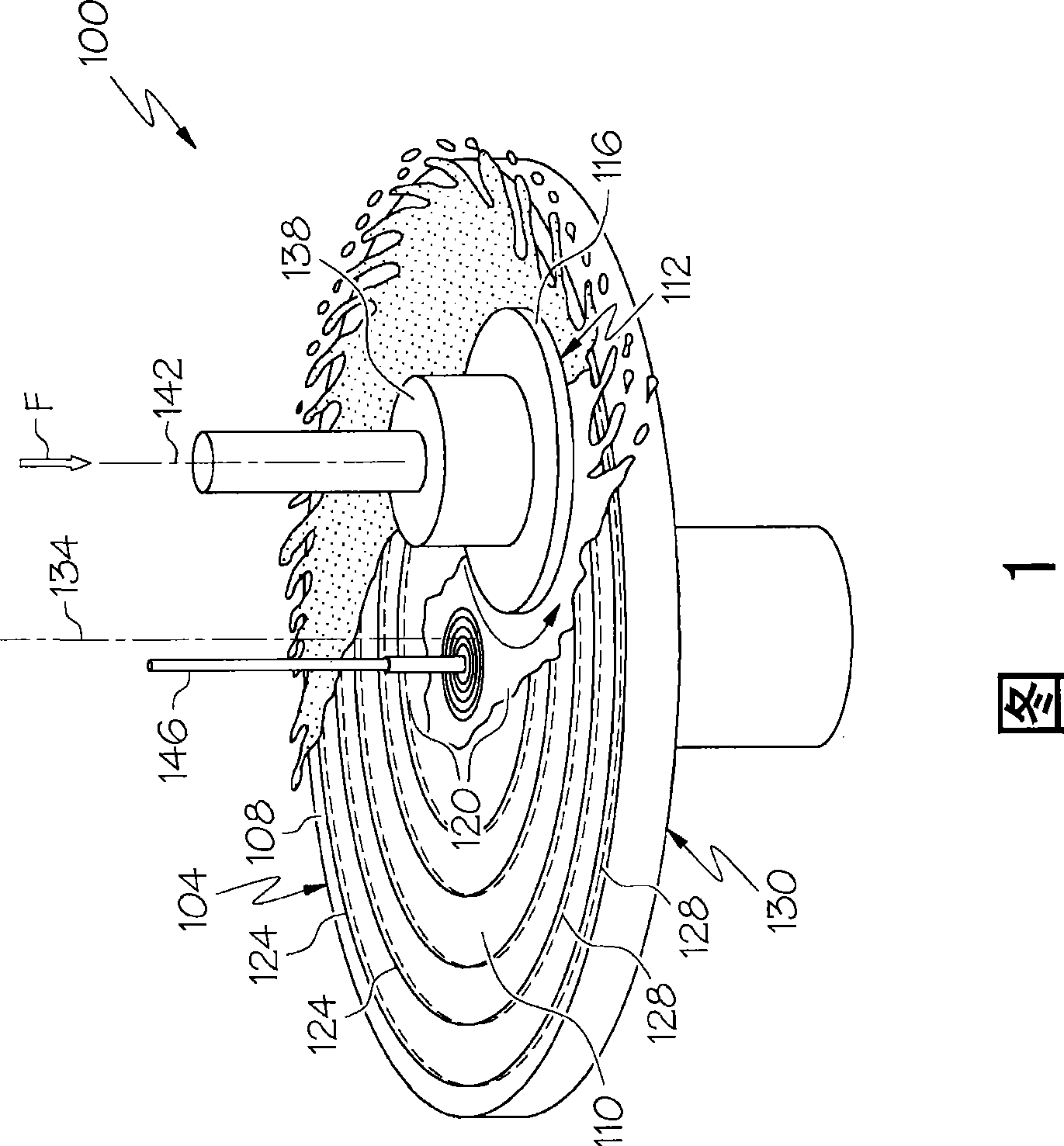
[0031] As used herein and in the appended claims, the term "hydrodynamic layer" refers to a region of the polishing layer immediately adjacent to the polishing surface that is substantially free of co-continuous fugitive phases.
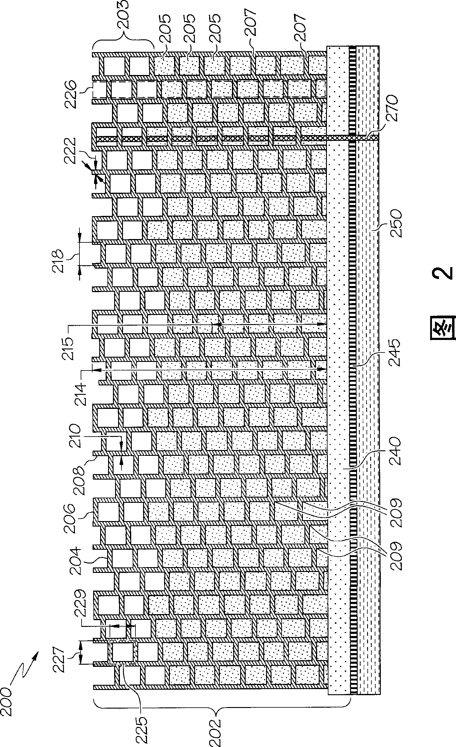
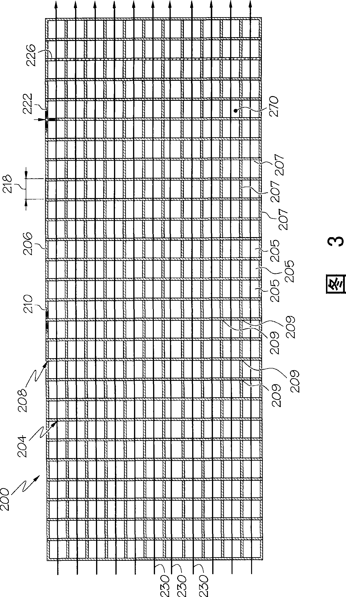
[0032] The term "interpenetrating network" as used herein and in the appended claims refers to a network comprising a continuous durabl...
PUM
| Property | Measurement | Unit |
|---|---|---|
| Depth | aaaaa | aaaaa |
Abstract
Description
Claims
Application Information