Micro-electroforming apparatus

A technology of micro-electroforming and electroforming liquid, applied in electroforming, electrolysis process, etc., can solve the problems of difficulty in solving the uniformity of the device microstructure on the wafer, not considering the electric field distribution of the wafer, and inconvenient operation, etc. The effect of electroplating quality, low production cost, and reduced workload

Inactive Publication Date: 2010-07-21
SHANGHAI JIAO TONG UNIV
View PDF1 Cites 3 Cited by
  • Summary
  • Abstract
  • Description
  • Claims
  • Application Information

AI Technical Summary

Problems solved by technology

However, this kind of device is very cumbersome to install and hang when it is necessary to monitor the thickness of the coating and perform multiple tests during the electroplating process, and it is inconvenient to operate.
Moreover, since the electric field distribution on the wafer is not considered, and the necessary auxiliary structures are introduced, it is difficult to solve the uniformity of the device microstructure on the wafer.

Method used


Image

  • Micro-electroforming apparatus
  • Micro-electroforming apparatus
  • Micro-electroforming apparatus

Examples


Embodiment Construction

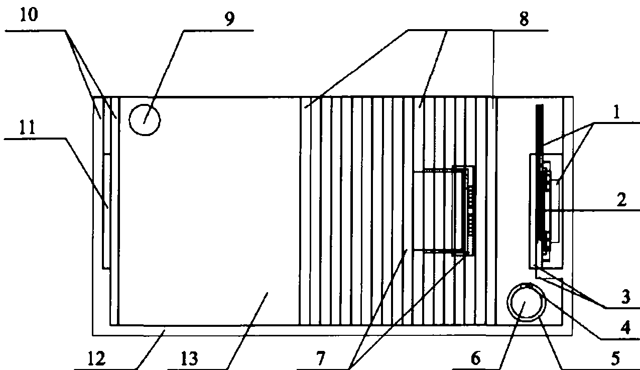
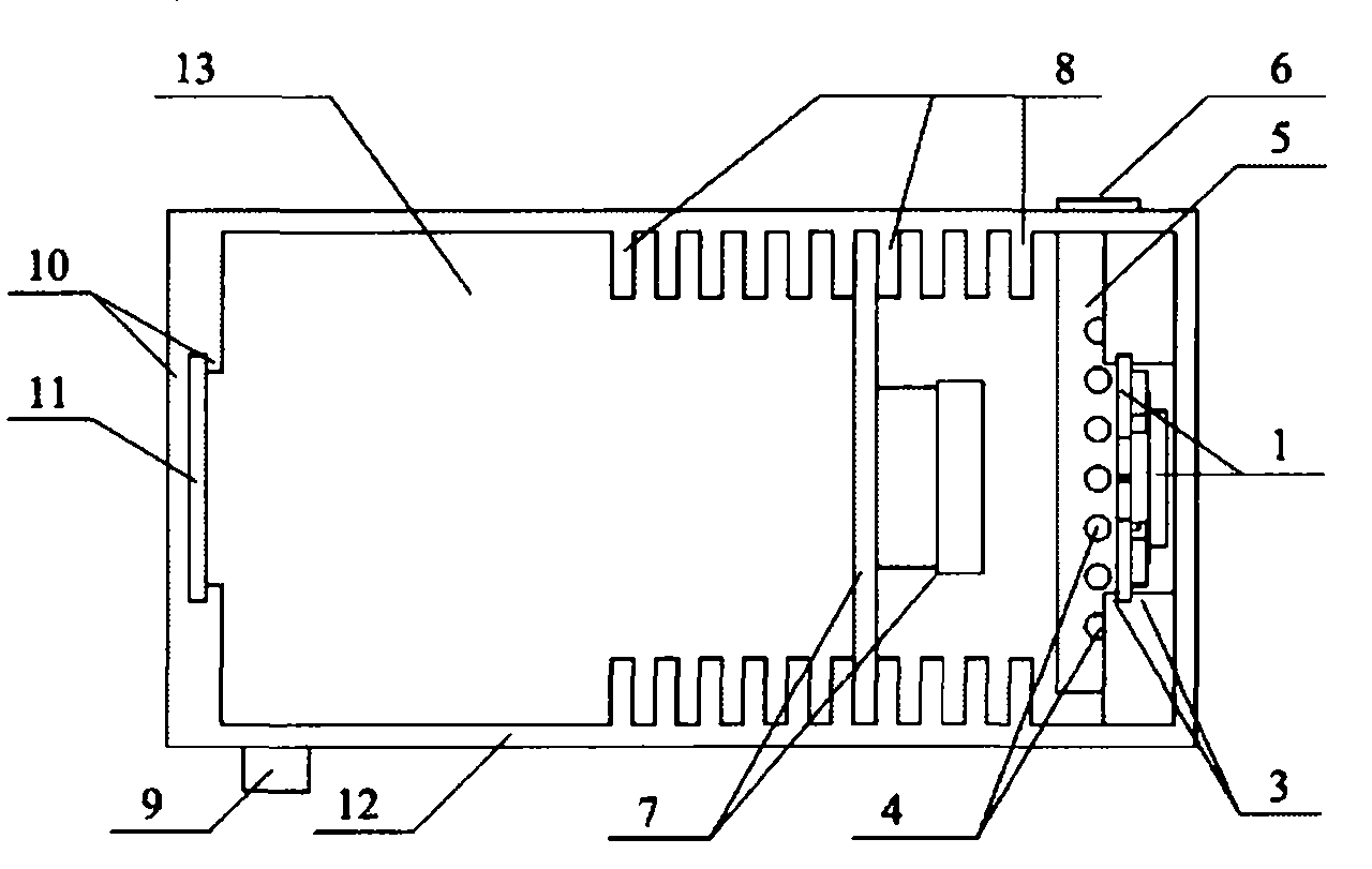
[0026] The embodiments of the present invention are described in detail below in conjunction with the accompanying drawings: this embodiment is implemented on the premise of the technical solution of the present invention, and detailed implementation methods and specific operating procedures are provided, but the protection scope of the present invention is not limited to the following the described embodiment.

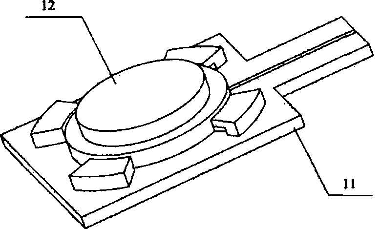
[0027] Such as figure 1 , 2 As shown, this embodiment includes: cathode fixture 1, cathode 2, electroforming liquid stirring tube 5, liquid inlet 6, electric field distribution baffle 7, electric field distribution baffle positioning baffle 8, liquid outlet 9, anode 11, Micro electroforming tank 12. The anode 11 and the cathode clamp 1 are vertically arranged on the side of the micro-electroforming tank 12 to face each other, the cathode 2 is placed in the cathode clamp 1, and the side plate of the micro-electroforming tank 12 is provided with an electroforming tank...


PUM


Abstract

The invention relates to a micro-electroforming device which comprises a cathode clamp, a cathode, an electroforming solution stirring pipe, a solution inlet, electric field distribution baffles, electric field distribution baffle positioning baffles, a solution outlet, an anode and a micro-electroforming bath. The anode and the cathode clamp are vertically arranged on the side surfaces of the micro-electroforming bath and face to each other; the cathode is arranged in the cathode clamp; the side plate of the micro-electroforming bath is provided with positioning baffles used for fixing the anode and the cathode clamp as well as a plurality of electric field distribution baffle positioning baffles; the electric field distribution baffles are arranged between the anode and the cathode; thesolution inlet is arranged below the side plate adjacent to the cathode; the electroforming solution stirring pipe is arranged right below the cathode and connected with the solution inlet. The solution outlet is arranged above the side plate adjacent to the anode. A plurality of sets of electric field distribution baffles in concentric circles as well as the circular auxiliary cathode before or on the front side of the cathode clamp make sure the electric fields are evenly distributed on a wafer, which realizes even thickness of MEMS device microstructure layers, convenient operation and high practicality.

Description

technical field [0001] The invention relates to a device in the technical field of micro-electromechanical systems (MEMS), in particular to a micro-electroforming device. Background technique [0002] Various micro devices that are small in size, light in weight, low in energy consumption and easy to mass-produce can be obtained by using MEMS (Micro Electro Mechanical Systems) technology. Among them, the LIGA (abbreviation of German Lithographie, Galvanoformung and Abformung) technology developed by Germany as a representative is a process technology that uses photolithography masks and electrochemical methods to realize the manufacture of three-dimensional non-silicon complex microstructures. It can be seen that micro-electroforming (plating) technology has become one of the key process technologies in the MEMS field. The basic principle of electroforming is the same as that of electroplating, which is based on electrochemical reactions. The biggest difference is the diffe...

Claims


Application Information

Patent Timeline
Patent Type & Authority Patents(China)
IPC IPC(8): C25D1/00
Inventor 汪红汤俊刘瑞王志民丁桂甫
Owner SHANGHAI JIAO TONG UNIV
Why Eureka
Try Eureka