Wafer transmission system

A chip transfer system and chip technology, applied in the direction of conveyor objects, transportation and packaging, etc., can solve the problems of affecting the output rate of the machine and reducing the processing capacity of the machine

Active Publication Date: 2009-03-11
BEIJING NAURA MICROELECTRONICS EQUIP CO LTD
View PDF0 Cites 20 Cited by
  • Summary
  • Abstract
  • Description
  • Claims
  • Application Information

AI Technical Summary

Problems solved by technology

[0009] First of all, the vacuum wafer aligner A' occupies the position of a target processing chamber PM, which reduces the processing capacity of the entire machine; secondly, the vacuum wafer aligner A' must be re-calibrated before each process, which affects the machine. output rate

Method used


Image

  • Wafer transmission system
  • Wafer transmission system
  • Wafer transmission system

Examples


Embodiment Construction

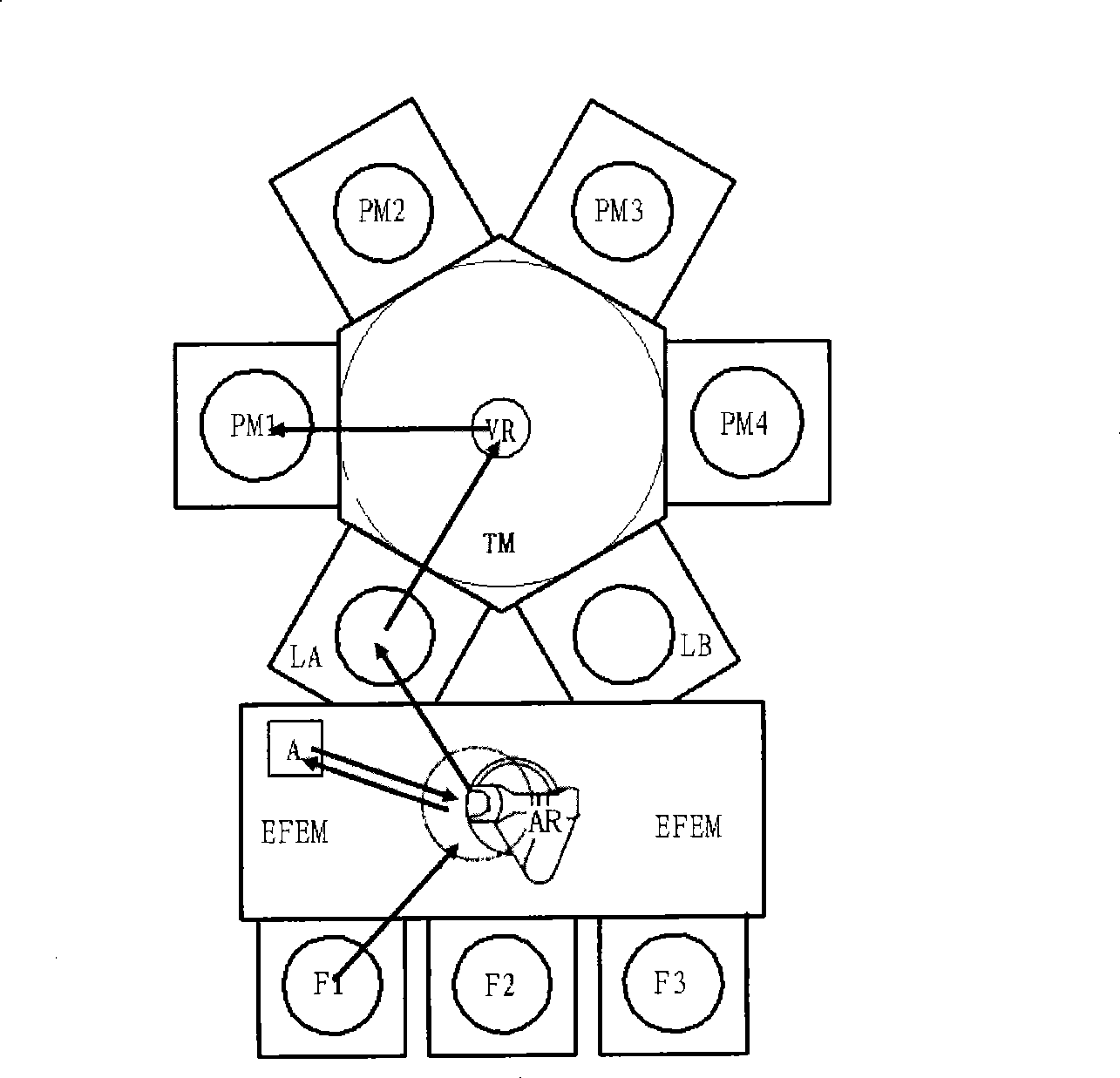
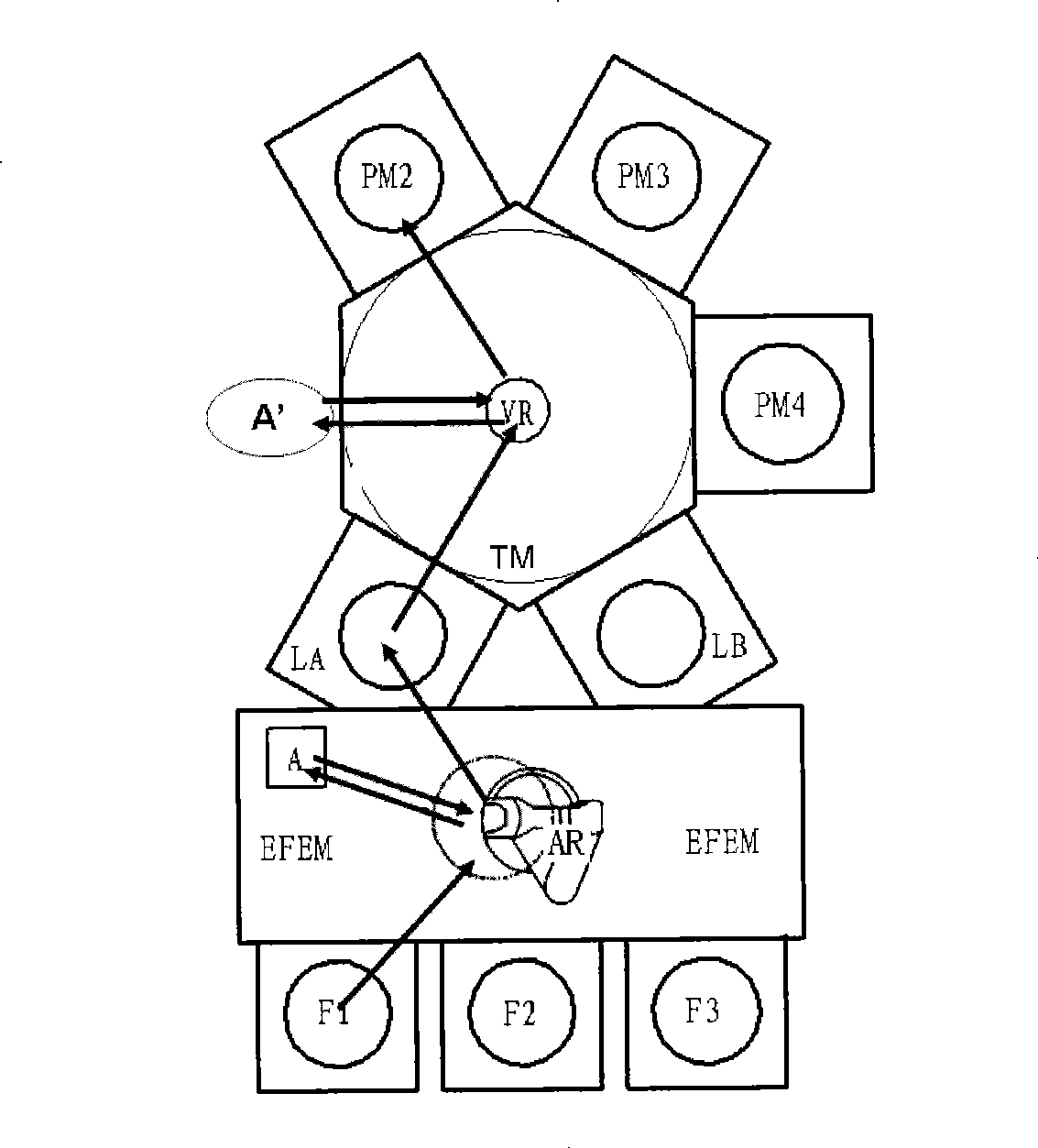
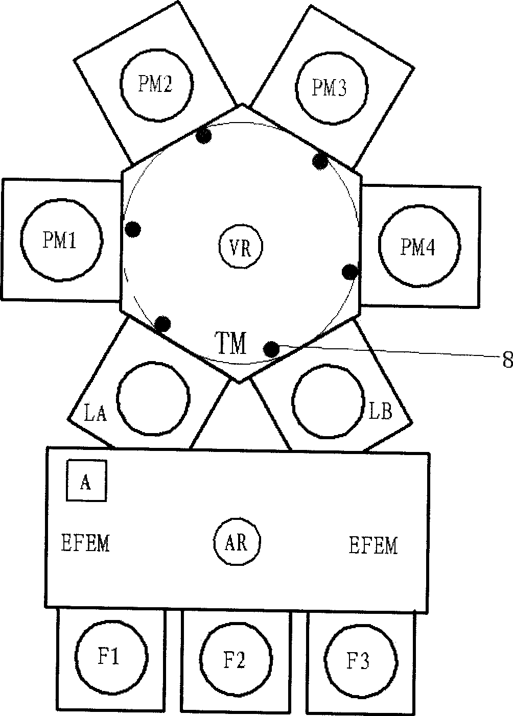
[0021] A preferred embodiment of the wafer transfer system of the present invention is as image 3 As shown, it includes a vacuum transfer chamber TM, and the vacuum transfer chamber TM is connected with multiple chambers, including target processing chambers PM1, PM2, PM3, PM4, vacuum transition load locks LA, LB, etc., which can also be connected as required other chambers.

[0022] The vacuum transfer chamber TM is equipped with a vacuum robot VR, which can transfer wafers between multiple chambers, and the wafer channel between the vacuum transfer chamber TM and each chamber is equipped with a sensor for sensing the position of the wafer 8. One or more sensors 8 can be provided at each wafer channel. When the wafer passes through the wafer channel, the sensor can perceive the position information of the wafer, and the transmission system can calibrate the position deviation of the wafer according to the information.

[0023] The sensor 8 can be a photoelectric sensor, an...


PUM


Abstract

The invention discloses a wafer transmission system which comprises a vacuum transmission cavity connected with a plurality of cavities, and each wafer channel which is arranged between the vacuum transmission cavity and each cavity is provided with an optical fibre sensor which is used for sensing the position information of a wafer; the optical fibre sensor comprises a transmitting terminal and a receiving terminal, a light which is transmitted by the transmitting terminal is perpendicular to the surface of the wafer, and the position of the optical fibre sensor slightly deflects to a center line of the wafer channel. When a vacuum mechanical arm is used for transmitting the wafer among the cavities, the position information of the wafer can be sensed by the sensor, the transmission system can calibrate the position bias of the wafer according to the position information, and the processing capability and the output rate of a mechanical table can not be influenced.

Description

technical field [0001] The invention relates to a semiconductor processing equipment, in particular to a wafer transmission system. Background technique [0002] In the semiconductor manufacturing process, the wafer transport system is connected to multiple wafer processing chambers. Wafers are transported from the warehouse to the processing chamber by the wafer handling manipulator through the wafer transfer system; and after the wafer processing is completed, the processed wafers are still transported back to the wafer warehouse by the manipulator through the wafer transfer system . [0003] With the reduction of the size and line width of the wafer processing process, the position accuracy of the manipulator placing the wafer in the processing chamber is also required to be higher and higher, so as to ensure the accuracy, repeatability and yield of wafer processing. At the same time, as the size of the wafer increases, the alignment accuracy of the wafer also increases...

Claims


Application Information

Patent Timeline
Patent Type & Authority Applications(China)
IPC IPC(8): H01L21/677
Inventor 张之山
Owner BEIJING NAURA MICROELECTRONICS EQUIP CO LTD
Why Eureka
Try Eureka