Nonvolatile memory structure and array thereof

A non-volatile memory and array technology, which is applied in the direction of electric solid-state devices, semiconductor devices, semiconductor/solid-state device components, etc., can solve the problems of reducing product production efficiency and product yield, short data storage time, and low read current interaction. Conduction and other issues, to achieve the effect of long data storage time, high reading current, and better mutual conductance

Inactive Publication Date: 2009-04-15
MACRONIX INT CO LTD
View PDF0 Cites 0 Cited by
  • Summary
  • Abstract
  • Description
  • Claims
  • Application Information

AI Technical Summary

Problems solved by technology

However, the above commonly used memories have disadvantages such as low read current, poor transconductance (GM), slow programming speed, and short data storage time in terms of electrical performance.
[0006] In addition, the silicon oxide isolation pattern located above the doped region needs to use complex manufacturing methods such as lift-off method, which will reduce the production efficiency and yield of products.

Method used


Image

  • Nonvolatile memory structure and array thereof
  • Nonvolatile memory structure and array thereof
  • Nonvolatile memory structure and array thereof

Examples


Embodiment Construction

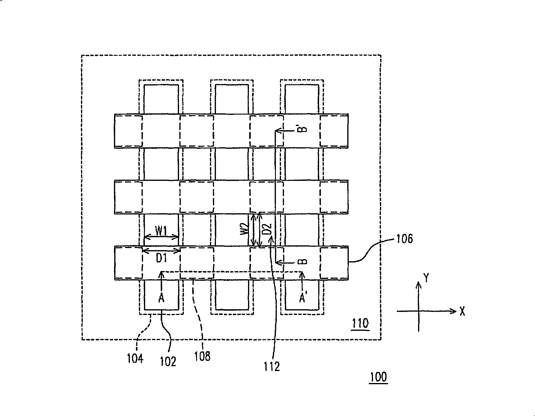
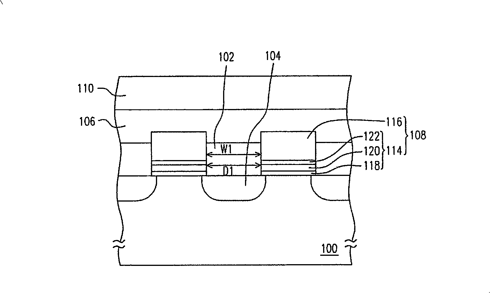
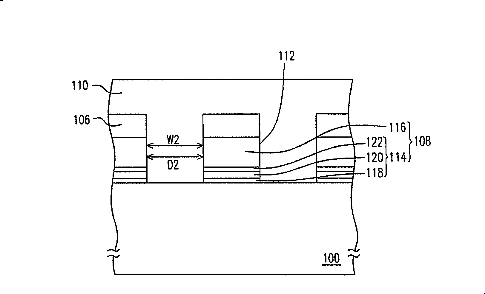
[0047] figure 1 What is shown is the top view of the nonvolatile memory arrays according to the first embodiment to the third embodiment of the present invention. figure 2 Shown are the first embodiment and the second embodiment of the present invention along figure 1 The cross-sectional view of the nonvolatile memory structure of the A-A' cross-section line in Fig. image 3 Shown are the first embodiment and the third embodiment of the present invention along figure 1 The cross-sectional view of the nonvolatile memory structure of the B-B' cross-hatching line. figure 1 The nonvolatile memory array includes a substrate 100 , isolation patterns 102 , doped regions 104 , word lines 106 , stack patterns 108 and a dielectric layer 110 . figure 2 The nonvolatile memory structure includes a substrate 100 , isolation patterns 102 , doped regions 104 , word lines 106 , stack patterns 108 and a dielectric layer 110 . image 3 The nonvolatile memory structure includes a substrate ...


PUM


Abstract

The invention relates to the technical field of non-volatile memories and discloses a non-volatile memory structure which comprises a substrate, multiple stack patterns and multiple stress patterns. The stack patterns are arranged on the substrate, and each stack pattern comprises a charge storage structure and a gate from bottom to top; wherein, the charge storage structure at least comprises a charge storage layer. The stress patterns are respectively arranged on the substrate between two adjacent stack patterns. The invention also discloses a non-volatile memory array. The non-volatile memory structure and non-volatile memory array effectively simplify the manufacturing process and improve the production efficiency of products. Furthermore, the non-volatile memory structure and the array thereof have better electrical property.

Description

technical field [0001] The invention relates to the technical field of nonvolatile memory, in particular to a nonvolatile memory structure and an array thereof. Background technique [0002] The electrically erasable programmable read only memory (electrically erasableprogrammable read only memory, EEPROM) in the non-volatile memory has the functions of storing, reading, erasing and writing data multiple times, and the stored data is It has the advantage of not disappearing later, so it has become a memory element widely used in personal computers and electronic equipment. [0003] A typical EEPROM uses doped polysilicon to make a floating gate (also known as a floating gate) and a control gate. When the memory is programmed, electrons injected into the floating gate are uniformly distributed throughout the polysilicon floating gate layer. [0004] In addition, there is also an EEPROM commonly used at present, which uses a charge trapping layer to replace the polysilicon f...

Claims


Application Information

Patent Timeline
Patent Type & Authority Applications(China)
IPC IPC(8): H01L27/115H01L23/528H01L27/11568
Inventor 古绍泓李士勤吴家伟林上伟韩宗廷陈铭祥吕文彬
Owner MACRONIX INT CO LTD
Why Eureka
Try Eureka