Radiation detector and radiation inspecting apparatus
A radiation detector and radiation technology, which are applied in measurement devices, radiation measurement, radiation intensity measurement, etc., can solve the problems of increased assembly cost, increased material cost, increased manufacturing cost, etc., so as to suppress the increase of manufacturing cost and maintain detection efficiency. , the effect of good spatial resolution
- Summary
- Abstract
- Description
- Claims
- Application Information
AI Technical Summary
Problems solved by technology
Method used
Image
Examples
no. 1 approach
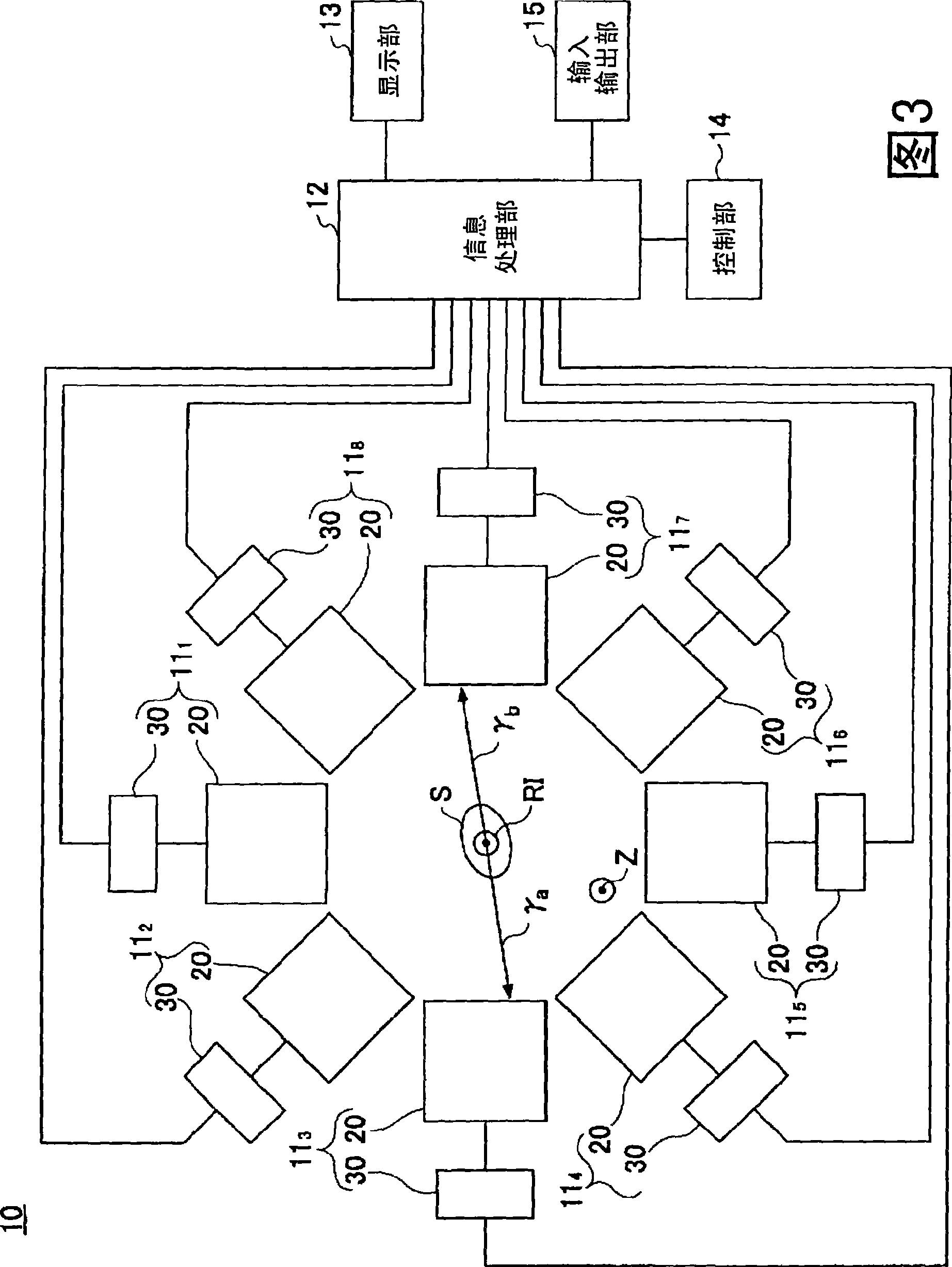
[0055] Fig. 3 is a block diagram showing the configuration of a PET apparatus according to the first embodiment of the present invention.
[0056] Referring to FIG. 3 , the PET apparatus 10 includes: a radiation detector 11 disposed around the subject S for detecting gamma rays; an information processing unit 12 processing the detection data from the radiation detector 11 and regenerating the obtained Image data of the position of the positron nuclide RI in the body of the subject S; the display unit 13, which displays the image data, etc.; the control unit 14, which controls the movement of the subject S or the radiation detector 11, etc.; and the output unit 15 , is composed of a terminal for sending instructions to the information processing unit 12 and the control unit 14, a printer for outputting image data, or the like.
[0057] The radiation detector 11 includes a semiconductor detection unit 20 and a detection circuit 30 . The semiconductor detection unit 20 is arrang...
no. 2 approach
[0096] Next, a PET apparatus according to a second embodiment of the present invention will be described. The PET apparatus related to the second embodiment is a modified example of the PET apparatus related to the first embodiment, and FIG. 4 and Figure 5 The illustrated semiconductor detection unit 20 is an example in which the number of semiconductor detection element arrays is expanded to n. The semiconductor detecting part of the second embodiment is the same as that shown in FIG. 4 and FIG. 4 except the number and arrangement of the semiconductor detecting element array. Figure 5 The illustrated semiconductor detectors are the same except for being different.
[0097] FIG. 9 is a schematic plan view of a semiconductor detection unit 40 constituting a PET device according to a second embodiment of the present invention. In the drawings, the same reference numerals (including reference numerals with different suffixes are also included) are attached to the parts corres...
PUM
 Abstract
Description
Claims
Application Information


