Multichannel amorphous silicon solar energy plate laser film-engraving machine
A technology of solar panels and solar panels, applied to lasers, nonlinear optics, laser welding equipment, etc., to achieve the effects of shortening processing time, saving investment, and simple structure
- Summary
- Abstract
- Description
- Claims
- Application Information
AI Technical Summary
Problems solved by technology
Method used
Image
Examples
Embodiment approach 1
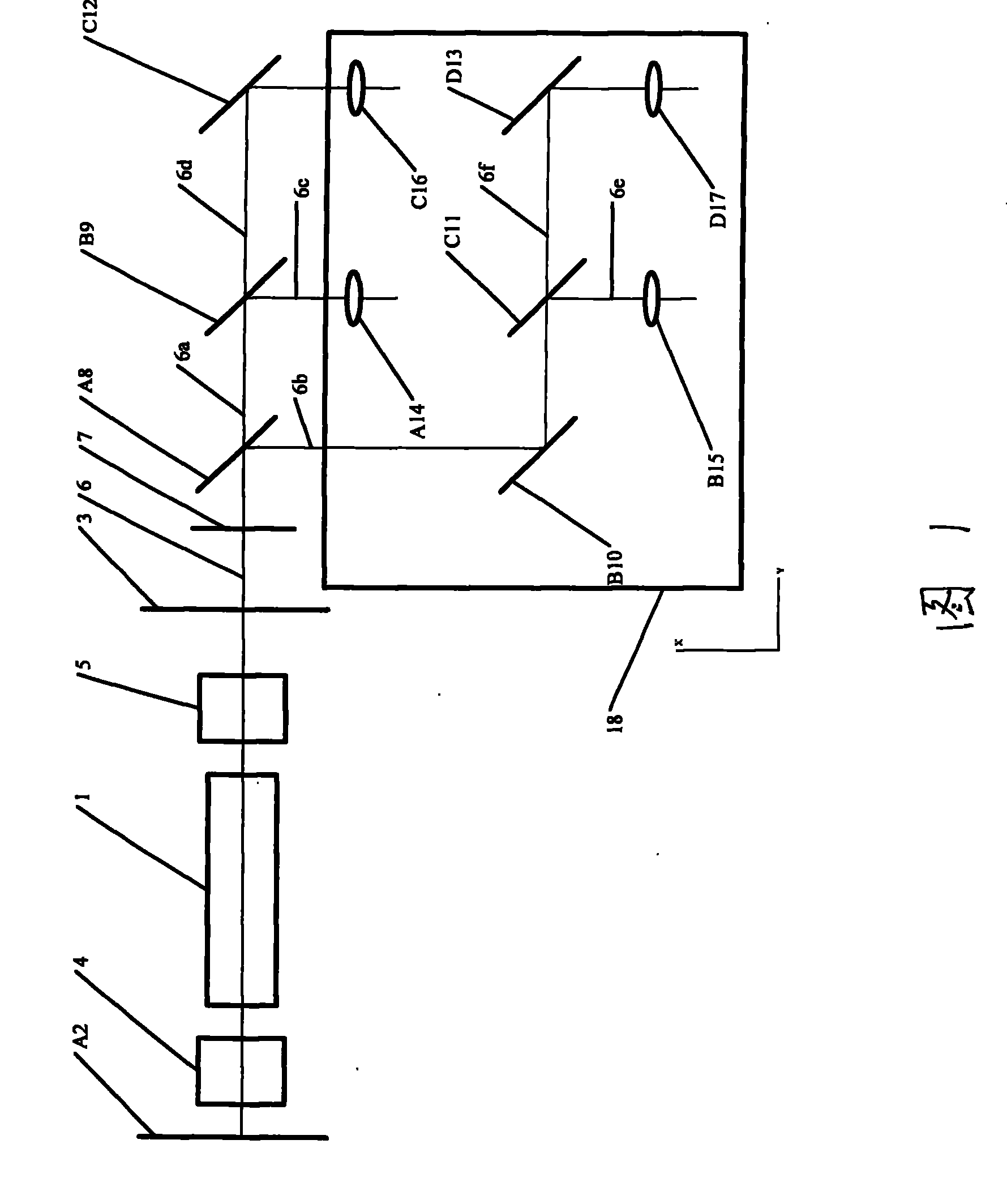
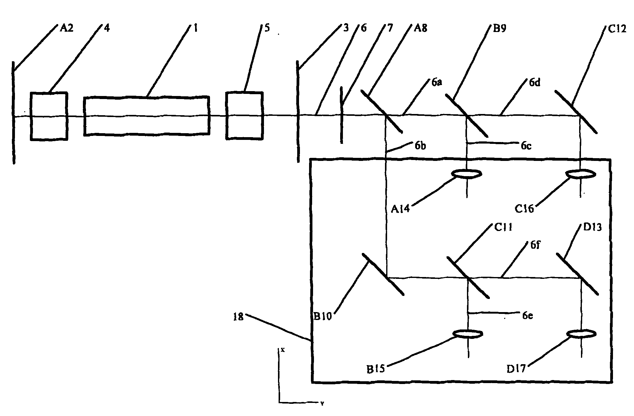
[0019] Implementation mode 1: if figure 1 As shown, a multi-channel amorphous silicon solar panel laser engraving machine adopts semiconductor-pumped YAG solid-state laser module 1, the laser power of this module is 50W, the laser wavelength is 1064nm, and the size of the YAG laser rod in the module is φ3-4 ×60-80mm, together with the 1064nm total reflection mirror A2, the 1064nm high reflection mirror 3, and the acousto-optic Q-switch 4 form a fundamental frequency 1064nm pulsed laser oscillation. The fundamental frequency laser is frequency-doubled by KTP crystal 5 (size 7×7×(7-12) mm, θ=90 degrees, φ=23.5-24.2 degrees) to generate frequency-doubled 532nm laser 6, 1064nm high reflection mirror 3 can transmit 532nm laser 6 at the same time. The frequency doubled laser light 6 is output from the high reflection mirror 3 .
[0020] The frequency-doubled laser beam 6 passes through a beam expander 7 (beam expansion ratio is 3-5) for beam expansion and collimation, and then pa...
Embodiment approach 2
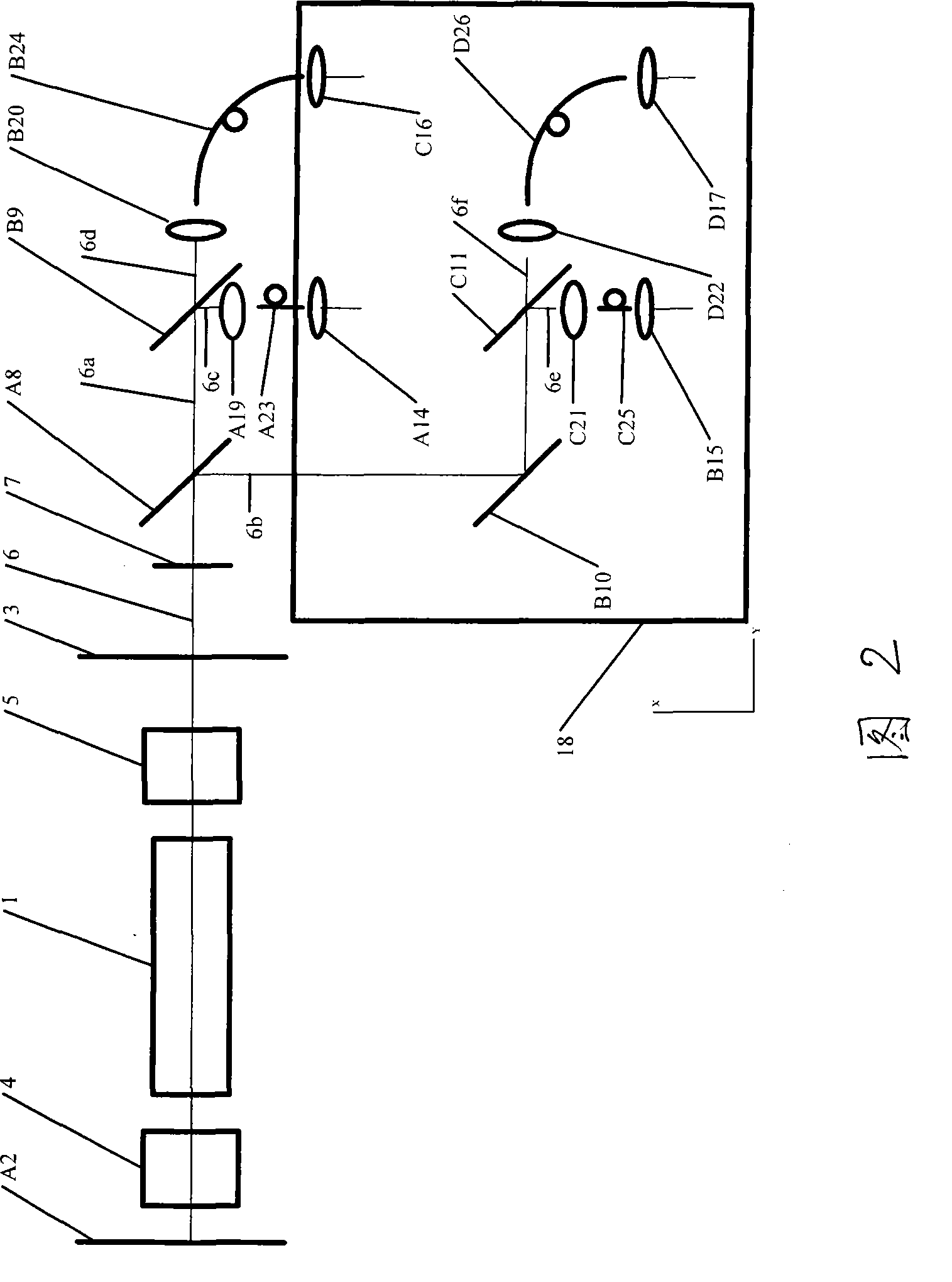
[0023] Implementation mode 2: if figure 2 As shown, the 4 laser beams 6c, 6d, 6e and 6f formed by the beam splitter B9 and the beam splitter C11 can also be coupled to the energy of 100-400 microns through the four coupling focusing systems A19, B20, C21 and D22 Among the optical fibers, after being transmitted by optical fibers A23, B24, C25, and D26, they reach four focusing lenses A14, B15, C16, and D17, which can also complete the task of multi-channel simultaneous processing.
[0024] The focal spot diameter of the multi-head laser output is 0.1mm, which can complete the scribing process of the conductive film of the solar cell and the photovoltaic layer, and the sum of the "three lines and two intervals" does not exceed 0.5mm.
PUM
 Abstract
Description
Claims
Application Information


