Wafer level encapsulation method of LED array encapsulation and LED encapsulation device made thereby

A technology of LED packaging and LED arrays, which is applied in the manufacture of electric solid-state devices, semiconductor devices, semiconductor/solid-state devices, etc., and can solve problems such as high cost, impossible high output, low-cost wafer-level packaging, and complex structures

Inactive Publication Date: 2009-05-20
THE HONG KONG UNIV OF SCI & TECH
View PDF0 Cites 22 Cited by
  • Summary
  • Abstract
  • Description
  • Claims
  • Application Information

AI Technical Summary

Problems solved by technology

[0004] This method is expensive due to its complex structure
Moreover, LED chips are individually packaged, which means that it is impossible to achieve high yield and low cost wafer level packaging

Method used


Image

  • Wafer level encapsulation method of LED array encapsulation and LED encapsulation device made thereby
  • Wafer level encapsulation method of LED array encapsulation and LED encapsulation device made thereby
  • Wafer level encapsulation method of LED array encapsulation and LED encapsulation device made thereby

Examples


Embodiment Construction

[0017] Hereinafter, preferred embodiments of the present invention will be described in detail with reference to the accompanying drawings. Referring now to the drawings, wherein the same reference numerals in different drawings represent the same or similar parts. In addition, known functions and structures that are considered unnecessary to the essential point of the present invention are not described in detail.

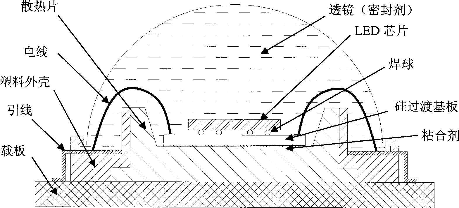
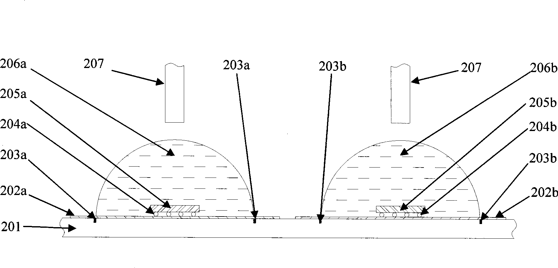
[0018] figure 2 A cross-sectional view of an embodiment of the invention is shown. The device shown in the figure includes a wafer 201, patterned conductive layers 202a and 202b, pre-etched grooves 203a and 203b, LED chips 205a and 205b with solder balls 204a and 204b, and a sealed seal deposited by an injection needle 207. Agents 206a and 206b.

[0019] The method of the present invention starts with a wafer 201 . The detailed process is as follows:

[0020] Step 1: Etching groove structures 203a and 203b on the wafer 201 by deep reactive ion etching (DRIE)...


PUM


Abstract

The invention discloses a wafer level packing method for packing LED array. In such a method, the LED chip array is first arranged on a crystal wafer that is provided with a socket in advance and can be used as a retention device of epoxide resin fluid in next packing process; then, the epoxide resin encapsulant is dripped on an underlay and then is solidified to finish the packing process. The usable LED can be obtained directly by cutting the wafer. Compared with the traditional technology, the wafer level packing method for packing LED array does not need moulds, thereby reducing cost and realizing high-density packing.

Description

Background of the invention [0001] Solid-state lighting (SSL) using high-brightness light-emitting diodes (HB-LEDs) is an emerging trend in general lighting applications. It is expected that in the next five to ten years, traditional incandescent and fluorescent lighting will be mostly replaced by solid-state lighting. There are currently two main factors inhibiting the popularity of HB-LEDs for solid-state lighting applications: one is their photoelectric efficiency, and the other is their cost. Both of these factors are closely related to the packaging of LEDs. Currently, almost all LEDs are packaged on single component substrates. The low throughput of this component-level packaging method makes it difficult to automate large-scale production, which is an important factor for low-cost manufacturing. Therefore, a more efficient packaging method is needed in the LED industry. [0002] current technology [0003] figure 1 A cross-sectional view of an LED packaging device...

Claims


Application Information

Patent Timeline
Patent Type & Authority Applications(China)
IPC IPC(8): H01L21/50H01L21/56H01L21/60H01L23/13H01L23/488H01L23/498H01L23/31H01L33/00
CPCH01L24/97H01L2924/10253H01L2224/48091H01L2924/181
Inventor 李世玮张荣
Owner THE HONG KONG UNIV OF SCI & TECH
Why Eureka
Try Eureka