
Manufacturing method for using compliant layer in grain reconfigured encapsulation construction

A technology of reconfiguration and packaging methods, applied in semiconductor/solid-state device manufacturing, electrical components, electrical solid-state devices, etc., can solve the problems of increasing the difficulty of cutting process, package warping, and inability to align

Active Publication Date: 2009-06-10
CHIPMOS TECH INC
View PDF2 Cites 2 Cited by
  • Summary
  • Abstract
  • Description
  • Claims
  • Application Information

AI Technical Summary

Problems solved by technology

This thinned die is reconfigured on another substrate, and then a plurality of dies are formed into a package package by injection molding; because the die is very thin, the package is also very thin , so when the package is detached from the substrate, the stress of the package itself will cause the package to warp, increasing the difficulty of the subsequent cutting process
[0006] In addition, after the wafer is diced, when it is reconfigured on another substrate, because the size of the new substrate is larger than the original size, it will not be aligned in the subsequent ball planting process, and the reliability of the packaging structure will be reduced.

Method used


Image

  • Manufacturing method for using compliant layer in grain reconfigured encapsulation construction
  • Manufacturing method for using compliant layer in grain reconfigured encapsulation construction
  • Manufacturing method for using compliant layer in grain reconfigured encapsulation construction

Examples


Embodiment Construction

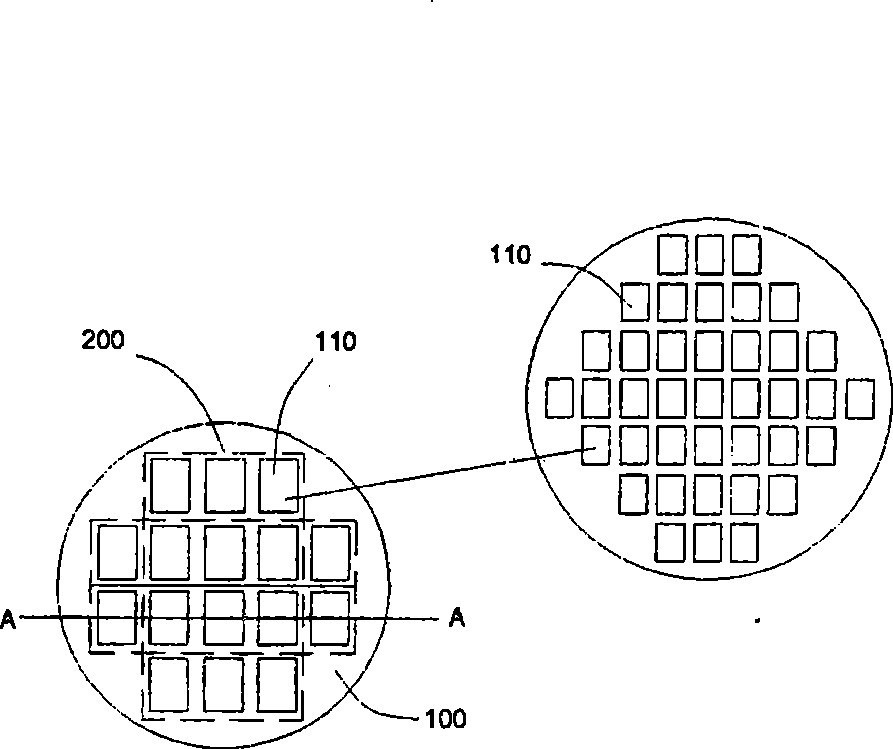
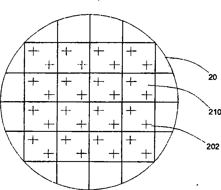
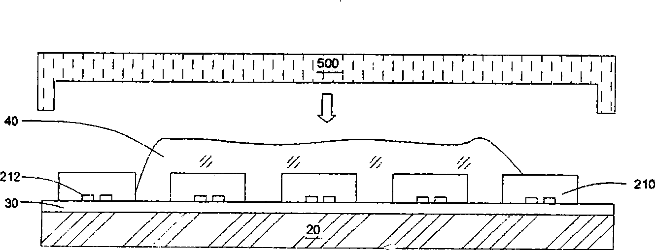
[0017] The direction of the present invention discussed here is a packaging method for reconfiguration of dies, a method of reconfiguring a plurality of dies on another substrate and then packaging them. In order to provide a thorough understanding of the present invention, detailed steps and components thereof will be set forth in the following description. Clearly, the practice of the invention is not limited to specific details of the manner in which chips are stacked, with which those skilled in the art are familiar. On the other hand, well-known chip formation methods and detailed steps of back-end processes such as chip thinning are not described in detail to avoid unnecessary limitations of the present invention. However, for the preferred embodiments of the present invention, it will be described in detail as follows, but in addition to these detailed descriptions, the present invention can also be widely implemented in other embodiments, and the scope of the present i...


PUM


Abstract

The invention relates to an encapsulation structure for reconfiguring crystal grains. The encapsulation structure comprises a crystal grain, an encapsulating body, a plurality of protrudent block structures, a plurality of patternized metal wire sections and a protective layer, wherein one active surface of the crystal grain is provided with a plurality of welding pads; the encapsulating body covers five sides of the crystal grain; the plurality of the protrudent block structures are formed from a macromelocular material and are arranged on the active surface of the crystal grain in an array mode; one end of each patternized metal wire section is in electric connection with the plurality of the welding pads on the active surface of the crystal grain; the other end of each patternized metal wire section extends and covers each protrudent block structure; and the protective layer is used for covering each patternized metal wire section and part of a patternized macromolecular material layer and exposing the protrudent block and the patternized metal wire section covered on the protrudent block structure.

Description

technical field [0001] The invention relates to a semiconductor packaging method, in particular to forming polymer bumps and metal layers on crystal grains to replace tin balls as conductive elements. Background technique [0002] Semiconductor technology has developed quite rapidly, so the miniaturized semiconductor die (Dice) must have diversified functional requirements, so that the semiconductor die must be configured with more input / output pads ( I / O pads), so that the density of metal pins (pins) has also increased rapidly. Therefore, the early lead frame packaging technology is no longer suitable for high-density metal pins; therefore, a ball array (Ball Grid Array: BGA) packaging technology has been developed. The ball array package has the advantage of higher density than the lead frame package. In addition, its solder balls are less prone to damage and deformation. [0003] With the popularity of 3C products, such as: cell phone (CellPhone), personal digital assi...

Claims


Application Information

Patent Timeline
IPC IPC(8): H01L21/50H01L21/60H01L21/56H01L23/485
CPCH01L2224/12105H01L24/19H01L2224/04105H01L2924/3025H01L2924/15174H01L24/96H01L2924/15311H01L24/20H01L21/6835H01L21/568H01L2224/0401H01L2224/19H01L2224/20H01L2924/3511
Inventor 吴佩宪
Owner CHIPMOS TECH INC
Learn More