Silicic double probe PMOS radiation dose meter based on insulator

A silicon-on-insulator and radiation dose technology, applied to dosimeters, etc., can solve the problems of dosimeters not working normally and being easily affected by external environmental factors, etc., and achieve the effects of repeated use, wide application range, and reduced production costs

Active Publication Date: 2009-06-17
SEMICON MFG INT (SHANGHAI) CORP +1
View PDF0 Cites 9 Cited by
  • Summary
  • Abstract
  • Description
  • Claims
  • Application Information

AI Technical Summary

Problems solved by technology

[0004] However, due to the semiconductor device nature of the PMOS dosimeter itself, it is easily affected by external environmental factors
The radiation sensitivity of PMOS dosimeters, the reliability and accuracy of long-term work in different environments, and the monitoring life are all key technologies to be solved urgently at present, and for PMOS dosimeters, for a specific process condition Its measurement tolerance can only be limited to a small range, and when the trapped charge in its oxide layer reaches saturation, the dosimeter will not work properly

Method used


Image

  • Silicic double probe PMOS radiation dose meter based on insulator
  • Silicic double probe PMOS radiation dose meter based on insulator
  • Silicic double probe PMOS radiation dose meter based on insulator

Examples


Embodiment Construction

[0041] In order to make the object, technical solution and advantages of the present invention clearer, the present invention will be described in further detail below in conjunction with specific embodiments and with reference to the accompanying drawings.

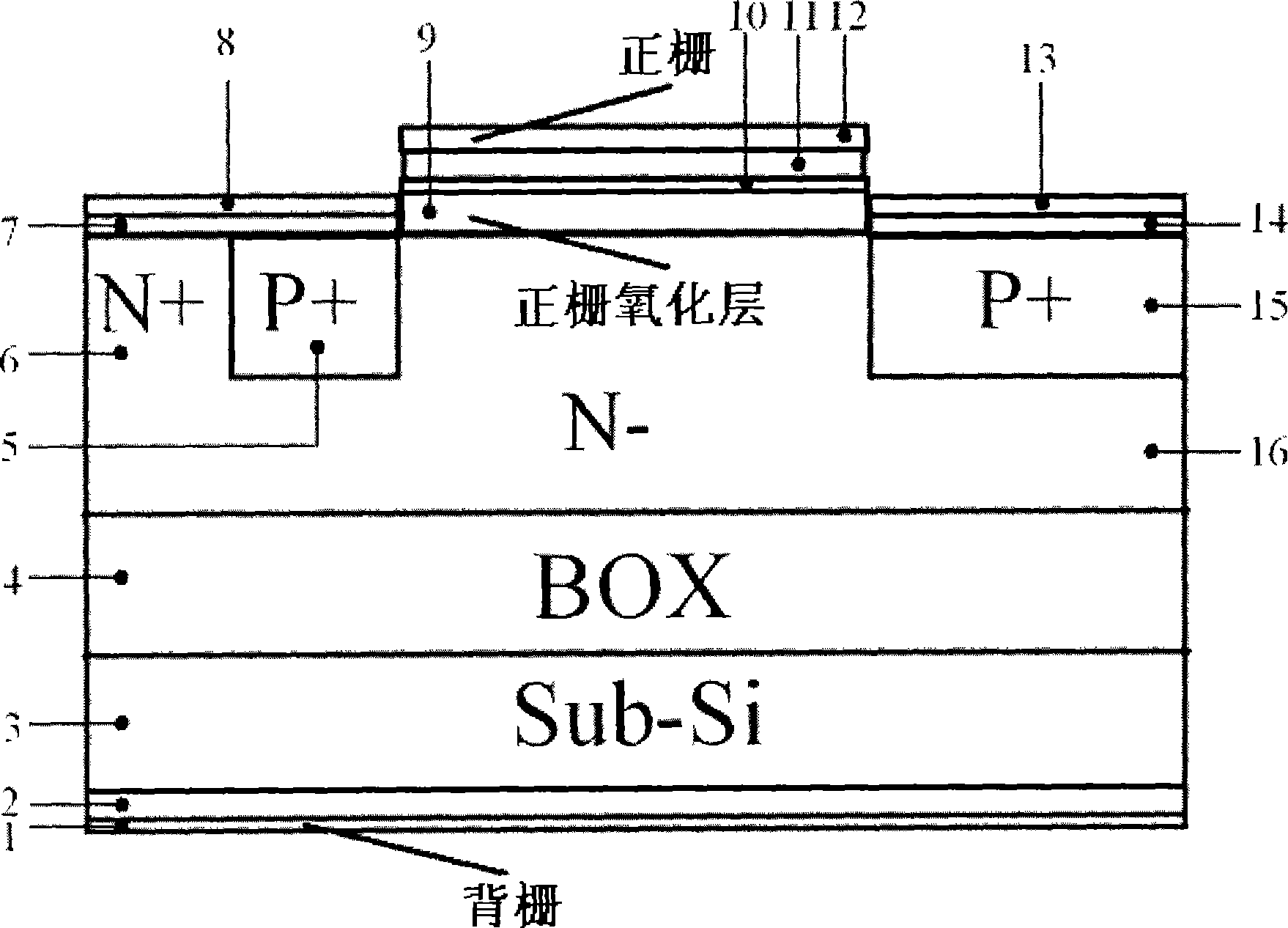
[0042] Such as figure 1 as shown, figure 1 It is a structural schematic diagram of the SOI-based dual-probe PMOS radiation dosimeter provided by the present invention. The radiation dosimeter uses the SOI of top silicon 16, buried oxide layer 4 and bottom silicon 3 as the basic structure from top to bottom. The radiation dose Count includes:

[0043] The positive gate oxide layer 9 disposed on the upper surface of the top silicon layer 16, the positive gate polysilicon layer 10 disposed on the upper surface of the positive gate oxide layer 9, the positive gate polysilicon layer 11 disposed on the upper surface of the positive gate polysilicon layer 10, and the positive gate polysilicon layer 11 disposed on the upper surf...


PUM


Abstract

The invention relates to the field of ionizing radiation dose measurement and discloses a PMOS radiation dosimeter which is based on SOI technology and can be recycled. The radiation dosimeter comprises a back-gate electrode, a multicrystalline silicide layer, a semiconductor substrate, a buried oxide layer, a toplevel silicon film, a body contact zone, a source zone, a drain region, a source electrode, a drain electrode, a front gate oxide, a front gate polycrystalline silicon layer and a front gate electrode. In the invention, the dosimeter is manufactured on an SOI substrate and is provided with two electrode probes to measure different dose rates; tuned-grid injections of a front gate and a back gate with different modes are adopted to adjust the measurement range of the probe; a high doping region which has the same shape as the toplevel silicon film is utilized to form the body contact which is short connected with the source zone; source/body, drain/body, the front gate and the back gate are connected with the respective electrode by the multicrystalline silicide; the front gate adopts a plurality of grid bars which are connected in parallel in an interdigital mode to enlarge the sensitive zone of the probe; the invention also provides annealing process control, bias condition, annealing temperature and time control and a circuit measuring method and a structure of a stacking dosimeter capable of adjusting the measuring range.

Description

technical field [0001] The invention relates to the technical field of ionizing radiation dose measurement, in particular to a dual-probe PMOS radiation dosimeter based on silicon-on-insulator. Background technique [0002] Research on the space radiation environment began in the 1940s. With the discovery of the strong radiation belt (Van-Allen belt) formed by the earth’s magnetic field capturing charged particles and the successive failures of satellite operations caused by radiation, more and more attention has been paid to the study of the space radiation environment. Various space radiation detection technologies and equipment It has been applied successively, including some technologies for total radiation dose monitoring, such as thermoluminescence (TLD) dosimeter, nylon film dosimeter, G-M counting tube, PIN diode, semiconductor detector, etc. Although these technologies have achieved some success, they also have their own defects. For example, it is difficult to re...

Claims


Application Information

Patent Timeline
Patent Type & Authority Applications(China)
IPC IPC(8): G01T1/02
Inventor 刘梦新韩郑生赵超荣刘刚
Owner SEMICON MFG INT (SHANGHAI) CORP
Why Eureka
Try Eureka