Shallow groove isolation construction manufacturing method

A technology of isolation structure and manufacturing method, applied in semiconductor/solid-state device manufacturing, electrical components, circuits, etc., can solve the problem of affecting the insulating isolation performance of shallow trench isolation structure, affecting the adhesion performance of dielectric material and trench 340, sidewalls, etc. and bottom etching damage, to achieve the effect of improving stability, enhancing adhesion, and reducing leakage current

Inactive Publication Date: 2009-06-17
SEMICON MFG INT (SHANGHAI) CORP
View PDF1 Cites 39 Cited by
  • Summary
  • Abstract
  • Description
  • Claims
  • Application Information

AI Technical Summary

Problems solved by technology

[0010] However, in the manufacturing process of the shallow trench isolation structure, such as image 3 In the dry etching process shown, the dry etching plasma is performing back etching (Pull Back Etch) on the second dielectric layer 330, the hard mask layer 320, and the pad silicon oxide layer 310 near the edge of the trench 340. At the same time, the sidewall and bottom of the trench 340 will also be etched, causing etching damage to the sidewall and bottom of the trench 340, which will affect the dielectric material and trench filling in the trench 340 in the subsequent process. The adhesion performance between 340 will affect the insulation isolation performance of the formed shallow trench isolation structure

Method used


Image

  • Shallow groove isolation construction manufacturing method
  • Shallow groove isolation construction manufacturing method
  • Shallow groove isolation construction manufacturing method

Examples


Embodiment Construction

[0049] The specific embodiments of the present invention will be described in detail below in conjunction with the accompanying drawings.

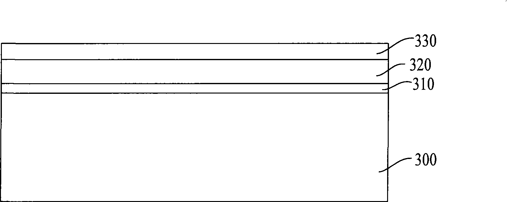
[0050] The shallow trench isolation structure is used to isolate semiconductor devices on the semiconductor substrate, and is formed by forming a trench on the semiconductor substrate and filling the trench with a dielectric material.

[0051] Please refer to Image 6 As shown, the manufacturing method of shallow trench isolation in the embodiment of the present invention is as follows:

[0052] Execute step S100, first provide a semiconductor substrate, and sequentially form a first dielectric layer and a hard mask layer on the semiconductor substrate;

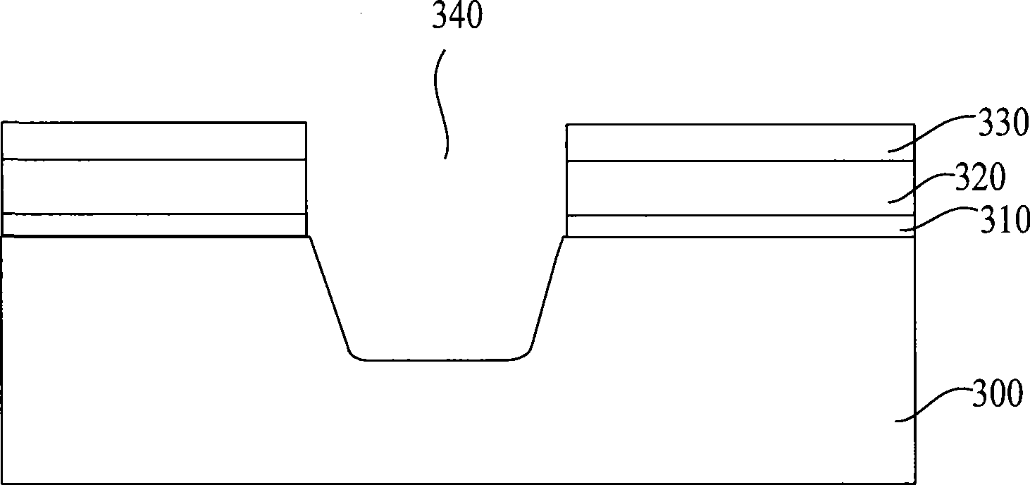
[0053] Execute step S110, and then, form an opening penetrating through the hard mask layer and the first dielectric layer in the hard mask layer and the first dielectric layer, and form a trench in the semiconductor substrate at the bottom of the opening;

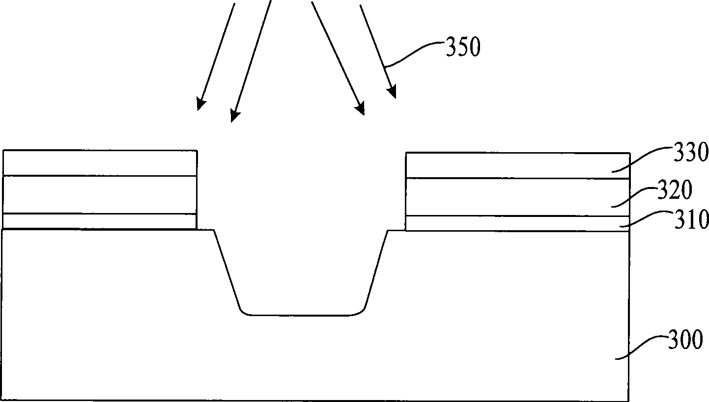
[0054] Execute step S120, an...


PUM


Abstract

A manufacturing method of a shallow trench isolation structure comprises steps of sequentially forming a first dielectric layer and a hard mask layer on a semiconductor substrate, arranging an opening which penetrates through the hard mask layer and the first dielectric layer and forming a trench in the semiconductor substrate at the bottom of the opening, forming a silicon oxide layer on the inner wall of the trench, etching the hard mask layer on the lateral wall of the opening and keeping the line width of the opening in the hard mask layer to be larger than that of the top portion of the trench, filling a second dielectric layer in the trench and the opening, and finally removing the hard mask layer and the first dielectric layer. The manufacturing method of a shallow trench isolation structure can not damage the lateral wall and the bottom of the trench when the hard mask layer is etched back.

Description

technical field [0001] The invention relates to the technical field of semiconductor manufacturing, in particular to a method for manufacturing a shallow trench isolation structure. Background technique [0002] With the increasing progress of semiconductor integrated circuit manufacturing technology, the line width of semiconductor devices in semiconductor integrated circuits is getting smaller and smaller, and the integration level is getting higher and higher. The traditional isolation process for semiconductor devices can no longer meet the continuous development of integrated circuit manufacturing. Process needs. [0003] At technology nodes of 0.35um and smaller, the industry uses a shallow trench isolation (Shallow Trench Isolation) process to achieve isolation between semiconductor devices. The main steps of the shallow trench isolation process are as follows: first, a trench is formed on a semiconductor substrate for manufacturing semiconductor devices, and then an...

Claims


Application Information

Patent Timeline
Patent Type & Authority Applications(China)
IPC IPC(8): H01L21/762
Inventor 何学缅王荣王丹
Owner SEMICON MFG INT (SHANGHAI) CORP
Why Eureka
Try Eureka