Circuit board manufacturing method and circuit board

A circuit board production, circuit board technology, applied in the direction of printed circuit manufacturing, printed circuit, printed circuit components, etc., can solve the problem of hole filling depression, unable to adapt to the production requirements of high-order blind holes or buried holes, and affect the quality of circuit boards, etc. problem, to achieve the effect of eliminating the hole filling depression

Inactive Publication Date: 2009-06-17
AVARY HLDG (SHENZHEN) CO LTD +1
View PDF0 Cites 10 Cited by
  • Summary
  • Abstract
  • Description
  • Claims
  • Application Information

AI Technical Summary

Problems solved by technology

[0005] However, when the existing manufacturing method is used to fill the guide hole, due to the gravitational effect of the filling material or the volatilization of the solvent in the filling material, etc., it is easy to generate a hole filling depression 110 at the guide hole, such as figure 1 shown
Due to the generation of hole filling depressions 110, the existing hole filling technology cannot meet the needs of the production of multi-layer high-density circuit board guide holes, especially the production requirements of high-order blind holes or buried holes, which will affect the quality of the circuit board
For example, if the hole filling depression 110 exists on the signal line of a multilayer high-density circuit board product, it may affect the transmission of the signal; Manufacturing precision of high-order guide holes
In addition, the appearance of filling depressions will also cause the surface of the copper clad substrate to be uneven, resulting in uneven thickness of the copper layer on the surface, which is not conducive to the production of conductive lines

Method used


Image

  • Circuit board manufacturing method and circuit board
  • Circuit board manufacturing method and circuit board
  • Circuit board manufacturing method and circuit board

Examples


Embodiment Construction

[0017] The circuit board manufacturing method provided by the technical solution and the circuit board manufactured by the method will be further described in detail below in conjunction with the accompanying drawings and embodiments.

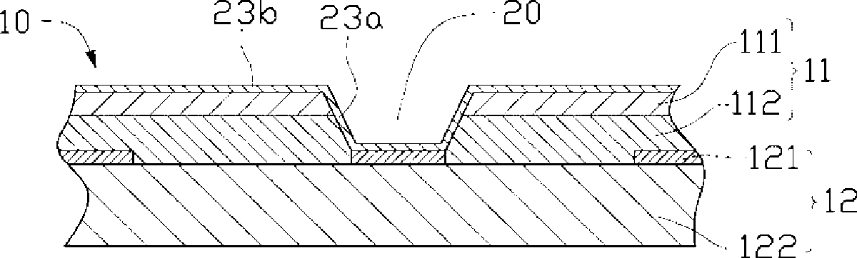
[0018] see figure 2 The circuit board manufacturing method provided in the embodiment of the technical solution includes the following steps:

[0019] In the first step, a copper-clad substrate 10 having at least one via 20 is provided.

[0020] The copper-clad substrate 10 has at least two copper layers and at least one resin layer between the at least two copper layers, so the copper-clad substrate 10 can be a single-layer double-sided copper-clad circuit substrate, It can also be a multi-layer circuit substrate that has completed internal circuit production and has not yet undergone surface circuit production. see figure 2 , in this embodiment, the copper-clad base material 10 is a multilayer circuit substrate, and the copper-clad base ...


PUM


Abstract

The invention provides a manufacture method for circuit board, which comprises providing a copper-coating base plate with at least a guide hole, connecting the conductive layer of the guide hole and a copper layer on the surface of the copper-coating base plate, filling the guide hole with filling material, arranging a guide hole baffle strip on the copper layer of the copper-coating base plate to completely cover the guide hole, micro-etching the copper layer of the copper-coating base plate outside the guide hole baffle strip to form a convex portion besides the guide hole which is filled with filling material, and removing the convex portion to ensure that the surface of filling material and the surface of the copper layer of the copper-coating base plate are in the same level. The invention also provides a circuit board made according to the method. The manufacture method for circuit board of the technical proposal effectively avoids pore depression of the guide hole during circuit board manufacture, ensures facial flatness of the copper-coating base plate, and reduces the depth of the copper layer of the copper-coating base plate, which benefits to manufacture high-density fine lines.

Description

technical field [0001] The invention relates to circuit board manufacturing technology, in particular to a circuit board manufacturing method and a circuit board manufactured by the method. Background technique [0002] With the development of electronic products in the direction of miniaturization and high speed, circuit boards are also developing from single-sided circuit boards and double-sided circuit boards to multi-layer high-density circuit boards. Multi-layer high-density circuit board refers to a circuit board with multi-layer conductive lines, which has more wiring area and higher interconnection density, so it is widely used. Please refer to Takahashi, A. et al. published in 1992 in IEEE Trans.on Components, Packaging, and Manufacturing Technology's document High density multilayer printed circuit board for HITAC M-880. [0003] The conductive lines of each layer of the multi-layer high-density circuit board are electrically connected through via holes. The guid...

Claims


Application Information

Patent Timeline
Patent Type & Authority Applications(China)
IPC IPC(8): H05K3/00H05K3/42H05K1/02
Inventor 苏莹林焕龙涂致逸黄伟
Owner AVARY HLDG (SHENZHEN) CO LTD
Why Eureka
Try Eureka