Method of manufacturing nitride semiconductor laser
A technology of nitride semiconductors and manufacturing methods, which is applied in the direction of semiconductor lasers, lasers, laser components, etc., can solve the problems that the film is easy to crack and the film is easy to be peeled off, and achieve the effect of reducing stress and reducing damage
- Summary
- Abstract
- Description
- Claims
- Application Information
AI Technical Summary
Problems solved by technology
Method used
Image

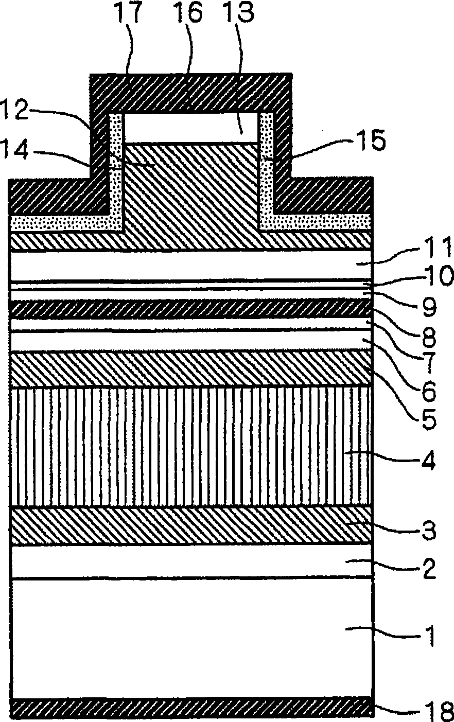
Examples
Embodiment 2
[0038] Embodiment 2 is characterized in that: when an ECR sputtering device is used to form an adhesive layer on the end face of the resonator, the RF power applied to the sputtering target is set to 2 levels of power, and the low-speed film-forming stage and the high-speed film-forming stage are used. The multi-level growth rate of the film stage is used to form the cohesive layer. Other methods are the same as in Example 1.
[0039] Figure 4 is a cross-sectional view of a resonator of a nitride semiconductor laser according to Embodiment 2 of the present invention. Such as Figure 4 As shown in FIG. The second adhesive layer 42 of the film is composed of a nitride dielectric. On the surface of the second adhesion layer 42, a low-reflection end surface coating film 43 is formed.
[0040] In addition, on the end face 44 of the resonator on the light reflection side, a first adhesive layer 45 made of a nitride dielectric that does not contain Ar is formed, and formed on t...
PUM
| Property | Measurement | Unit |
|---|---|---|
| length | aaaaa | aaaaa |
Abstract
Description
Claims
Application Information