Process for blind hole, buried hole, and filled hole of multi-layered high density interconnected printed circuit board

A high-density interconnection and printed circuit board technology, which is applied in the direction of multi-layer circuit manufacturing and electrical connection formation of printed components, can solve the problems of many process steps, improve production efficiency, save production process, and shorten production time Effect

Inactive Publication Date: 2009-07-08
HONGYUAN TECH HANGZHOU
View PDF3 Cites 19 Cited by
  • Summary
  • Abstract
  • Description
  • Claims
  • Application Information

AI Technical Summary

Problems solved by technology

[0019] The disadvantage of the above process is that there are many steps in the post-processing pro

Method used


Image

  • Process for blind hole, buried hole, and filled hole of multi-layered high density interconnected printed circuit board
  • Process for blind hole, buried hole, and filled hole of multi-layered high density interconnected printed circuit board

Examples


Embodiment Construction

[0029] specific implementation plan

[0030] The present invention will be further described below in conjunction with embodiment:

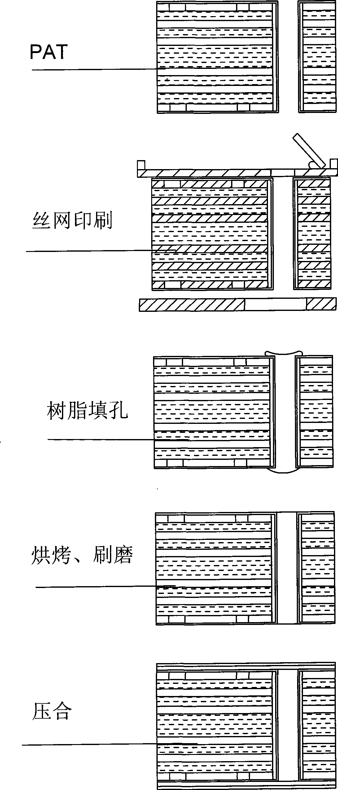
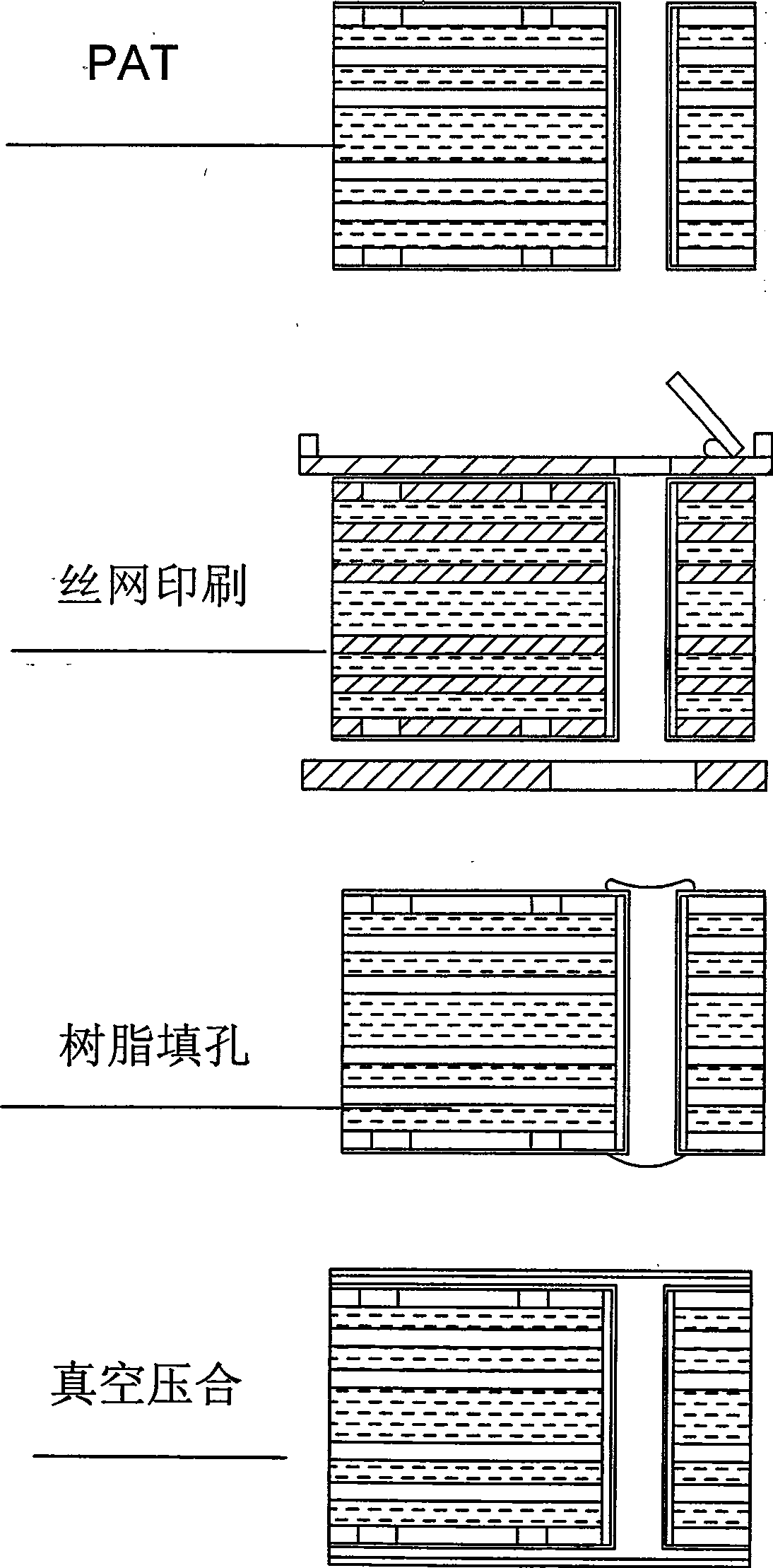
[0031] refer to figure 2 As shown, the blind hole, buried hole, and hole filling process of multilayer high-density interconnection printed circuit boards, (1) firstly use liquid medicine to generate uniform reddish brown or black oxidation on the copper surface of printed circuit boards with drilled holes. layer, so that the roughness of the oxide layer can be formed so that it can be tightly combined with the bonding sheet and can avoid the cuprous chloride formed by the high-temperature reaction between the surface of the raw copper and the pressing, which affects the reliability of the product. (2) followed by the traditional screen For printing, first drill the holes to be filled on the aluminum sheet, and then put the perforated aluminum sheet into the wooden screen frame instead of the traditional silk cloth screen, and use the aluminum ...


PUM


Abstract

The invention relates to a blind hole, buried hole, and porefilling craft for a multi-layer high-density interconnect printed circuit board, which is characterized in that the blind hole, buried hole, and porefilling craft for a multi-layer high-density interconnect printed circuit board firstly generates even brick red or black oxide layer on the copper surface of a printed circuit board provided with bores utilizing liquid medicine; with roughness of the generated oxide layer, the oxide layer can be closely connected with an adhesive tablet and can avoid an influence on reliability of the product from the surface of pig copper and cuprous chloride formed by a pressing high temperature reaction; then a traditional screen printing is carried out. The craft is characterized in that resin is filled into an appointed hole and laminating of the adhesive tablet is carried out within a time limit, then a vacuum compressing craft is carried out. The blind hole, buried hole, and porefilling craft for a multi-layer high-density interconnect printed circuit board can shorten the production labor hour and improve productivity.

Description

technical field [0001] The invention relates to circuit boards in the electronics industry, in particular to a process for filling blind holes and buried holes of multilayer high-density interconnected printed circuit boards. Background technique [0002] With the electronic industry's desire for increasingly light and compact products, and the increasing demand for complex functions, the upstream supply chain is forced to continue to develop and innovate, and to improve the technical level of the independent industry. [0003] As far as printed circuit boards are concerned, high-density interconnection technology has been developed since the early 1980s and has covered most of the application fields of the entire electronics industry, such as mobile phones, mobile personal computers, wireless network communication products, digital mobile phones, digital satellites, etc. How can the degree of industrial development of today's technological products such as navigation system...

Claims


Application Information

Patent Timeline
IPC IPC(8): H05K3/46H05K3/42
Inventor 林睦群
Owner HONGYUAN TECH HANGZHOU
Why Eureka
Try Eureka