Active component array substrate and method thereof
A technology of active components and substrates, applied in the fields of nonlinear optics, instruments, optics, etc., can solve the problems of occupying the space of the substrate 11, cannot be repaired, and the repair rate cannot be effectively improved, so as to save the layout area and improve the repair rate.
- Summary
- Abstract
- Description
- Claims
- Application Information
AI Technical Summary
Problems solved by technology
Method used
Image

Examples
no. 1 example
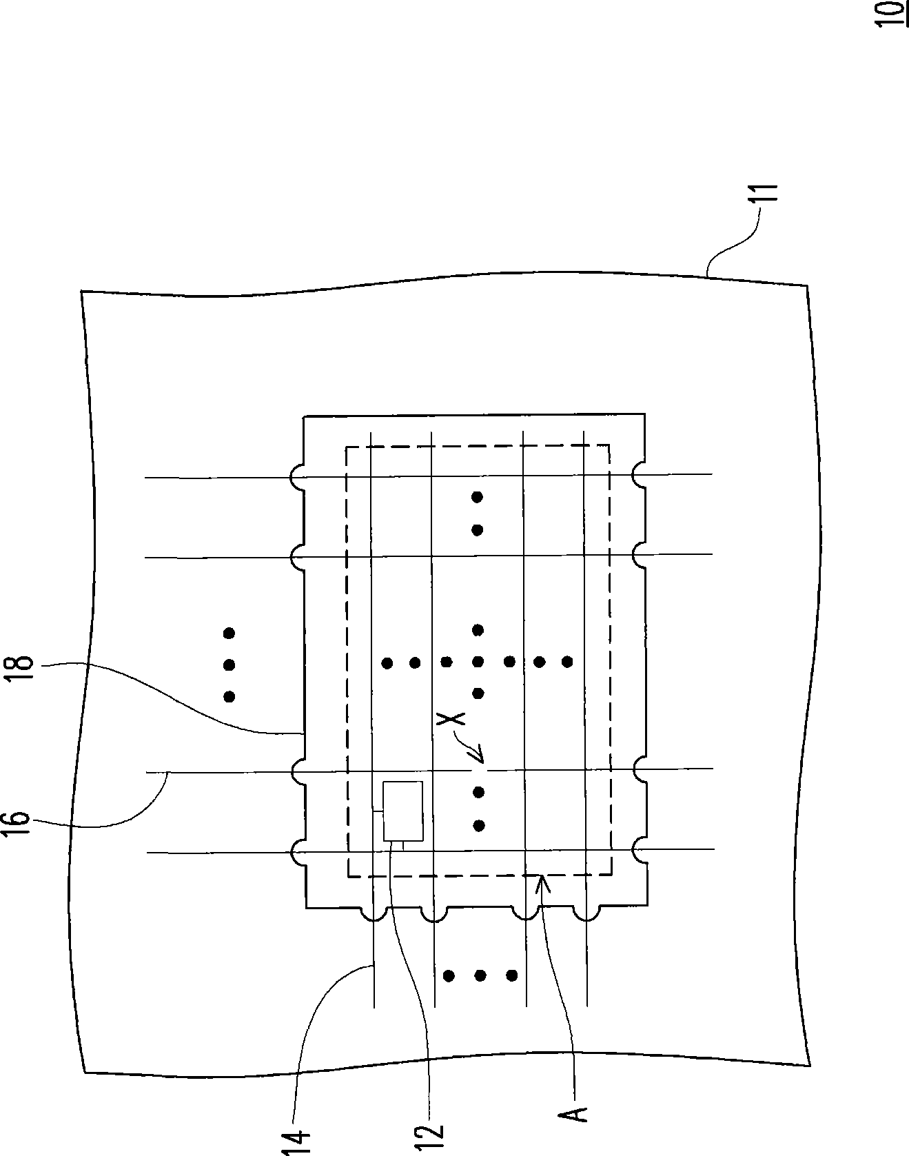
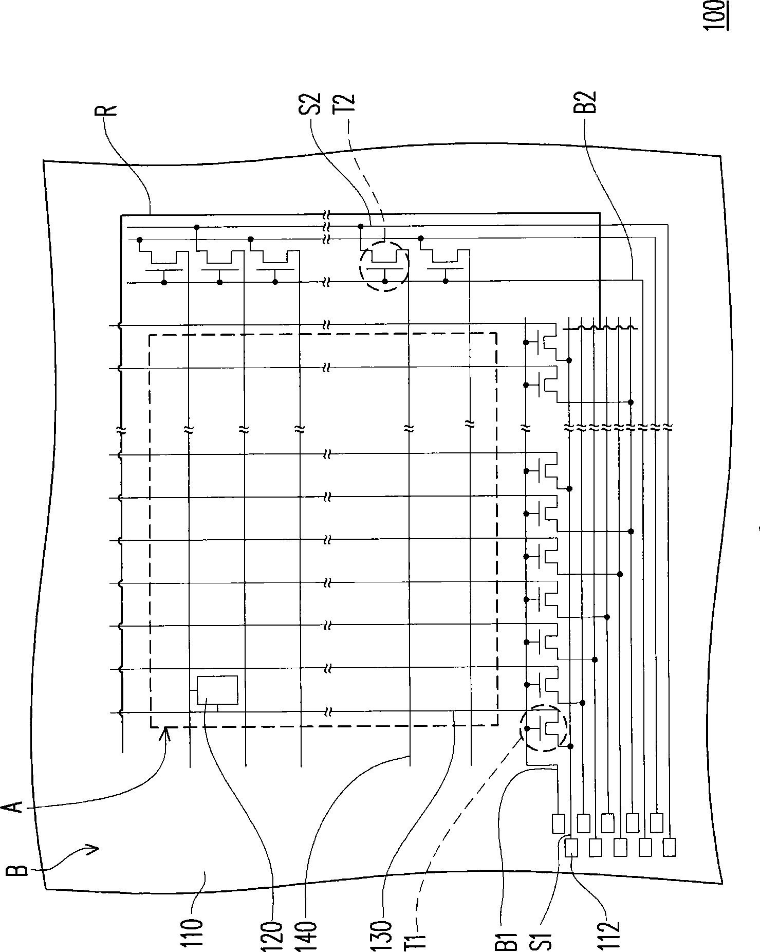
[0075] Figure 2A is a schematic diagram of the active component array substrate of the first embodiment of the present invention. Please refer to Figure 2A , the active component array substrate 100 of the present invention includes a substrate 110, a plurality of pixel units 120, a plurality of first signal lines 130, a plurality of second signal lines 140, a plurality of first shorting bars S1, and a plurality of first switch components T1, a first bus wire B1, at least one reconstruction rod R, a plurality of second short-circuit bars S2, a plurality of second switch components T2, and a second bus wire B2. The substrate 110 has an active area A and a peripheral circuit area B surrounding the active area A. As shown in FIG. The pixel unit 120 is disposed in the active area A and is electrically connected to the corresponding first signal line 130 and the second signal line 140 . Depend on Figure 2A It can be seen that both the first signal line 130 and the second sig...
no. 2 example
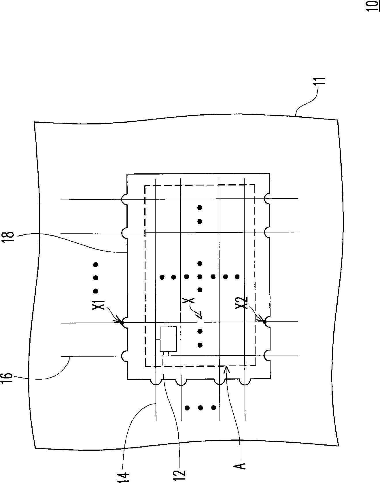
[0082] The second embodiment is similar to the first embodiment, and the similarities will not be repeated here. The main difference between the two is: the number of reconstruction rods. The active component array substrate of this embodiment includes a plurality of rebuilding rods. Figure 4A It is a schematic diagram of the active component array substrate of the second embodiment of the present invention. Please refer to Figure 4A , the active component array substrate 300 of this embodiment includes a plurality of reconstruction rods. One ends of these rebuilding rods R straddle the corresponding first shorting rods S1 respectively. In addition, the other end of the rebuilding rod R extends outward to cross over the end of the first signal line 130 not connected to the first switch component T1.
[0083] Figure 4B It is a schematic diagram of the repaired active component array substrate according to the second embodiment of the present invention. Please refer to ...
no. 3 example
[0085] The third embodiment is similar to the first embodiment, and the similarities will not be repeated here. The main difference between the two lies in the layout of the first reconstruction rod and the second reconstruction rod in this embodiment. Figure 5A is a schematic diagram of the active component array substrate of the third embodiment of the present invention. Please refer to Figure 5A , the active device array substrate 400 of this embodiment has a plurality of first reconstruction rods R1 and a plurality of second reconstruction rods R2. The first reconstruction rod R1 and the second reconstruction rod R2 are disposed in the peripheral circuit area B. In particular, one ends of the first rebuilding rods R1 straddle the corresponding first signal wires 130 respectively, and the other ends of the first rebuilding rods R1 extend outwards to straddle the corresponding second shorting rods S2 respectively. In addition, one end of the second rebuilding rod R2 cro...
PUM
 Abstract
Description
Claims
Application Information
 - R&D
- Intellectual Property
- Life Sciences
- Materials
- Tech Scout
- Unparalleled Data Quality
- Higher Quality Content
- 60% Fewer Hallucinations
Browse by: Latest US Patents, China's latest patents, Technical Efficacy Thesaurus, Application Domain, Technology Topic, Popular Technical Reports.
© 2025 PatSnap. All rights reserved.Legal|Privacy policy|Modern Slavery Act Transparency Statement|Sitemap|About US| Contact US: help@patsnap.com