Three-layer stereo power encapsulation method and structure
A packaging method and power technology, which is applied in the manufacture of semiconductor devices, electric solid devices, semiconductor/solid devices, etc., can solve the problems of power integration and packaging of IPM products, and achieve the effects of low cost, simplified production process, and easy welding
- Summary
- Abstract
- Description
- Claims
- Application Information
AI Technical Summary
Problems solved by technology
Method used
Image
Examples
Embodiment Construction
[0050] The technical solutions of the present invention will be further described in more detail in conjunction with the accompanying drawings and specific embodiments.
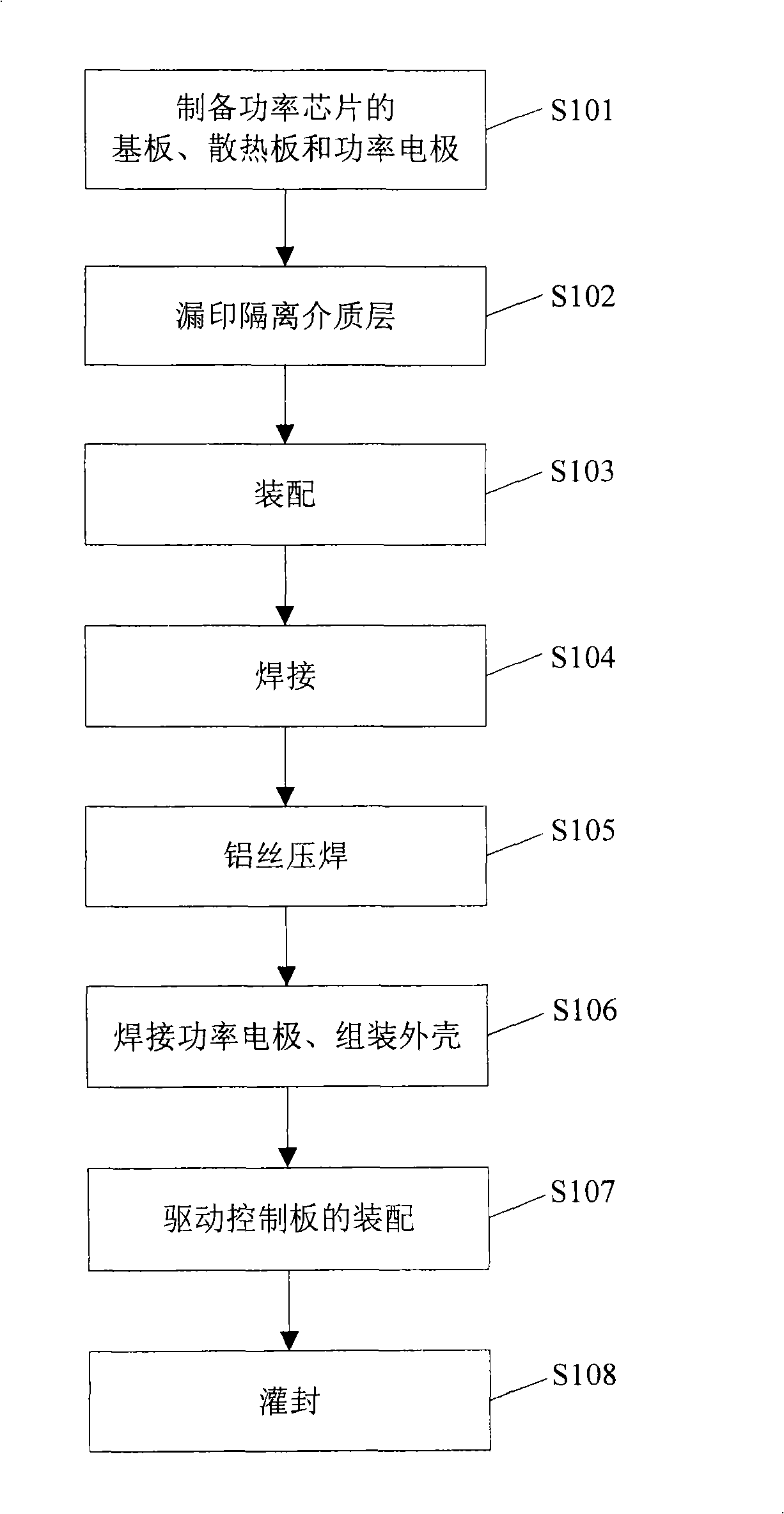
[0051] Such as figure 1Shown is the process flow diagram of the three-layer three-dimensional packaging method of the present invention. The method tightly installs the power board part, the drive control board part, and the power electrode part in a package from bottom to top, and the method includes the following steps:
[0052] Step S101, preparing the substrate of the power chip, the cooling plate and the power electrode;
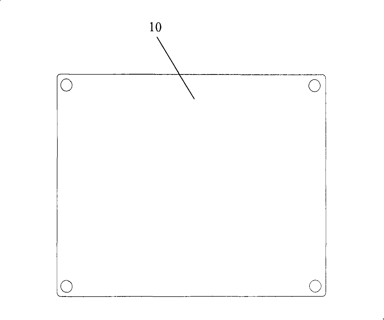
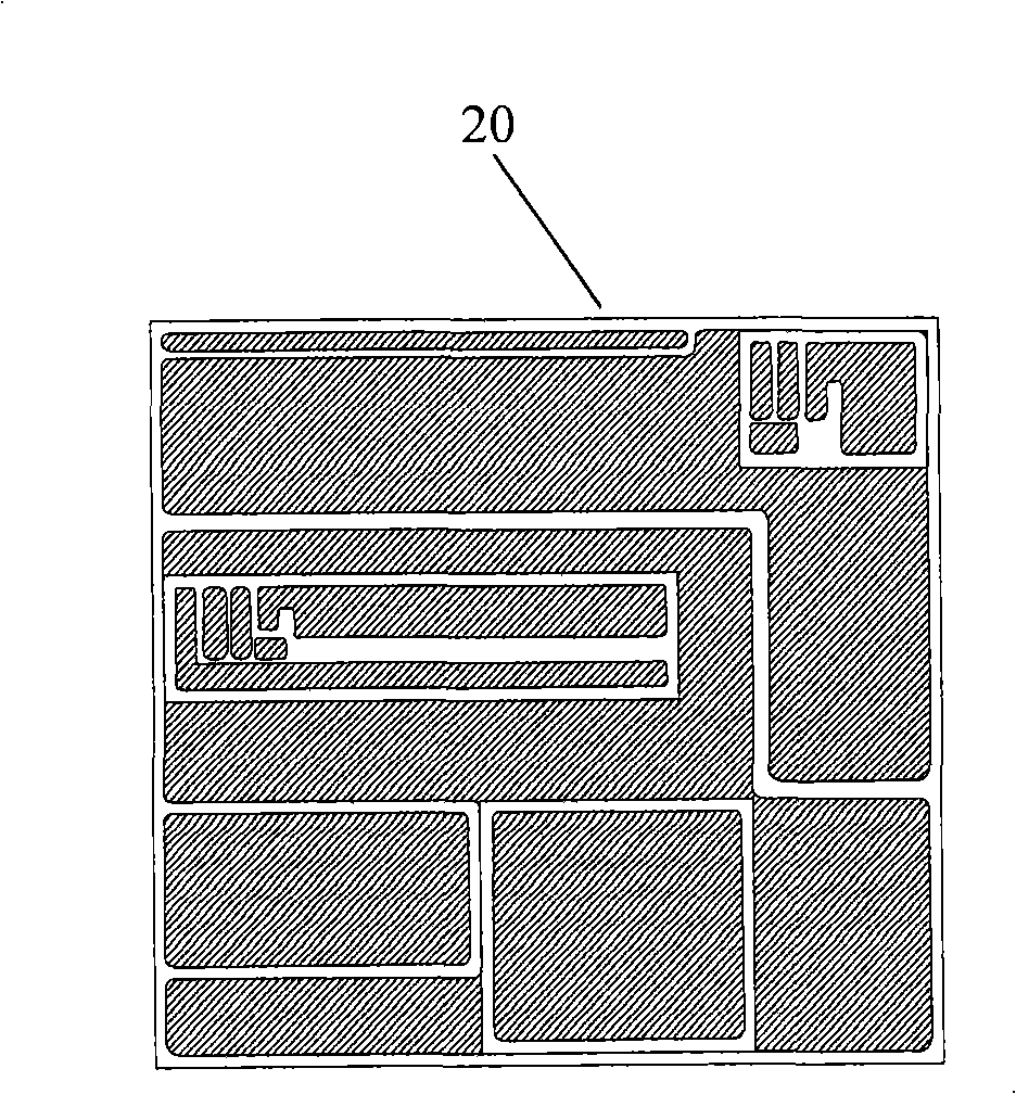
[0053] In this step, design and process the copper heat sink and power electrodes according to the required size; design and process the ceramic copper clad board (DCB) as the mounting substrate of the power chip according to the layout requirements of the power device, such as Figure 2a , Figure 2b , Figure 2c , Figure 6, wherein 10 is a copper heat sink, 20 is a ceramic copper...
PUM
 Abstract
Description
Claims
Application Information


