High voltage power fast recovery diode and manufacturing method thereof

A technology for recovering diodes and power, which is applied in the fields of final product manufacturing, sustainable manufacturing/processing, semiconductor/solid-state device manufacturing, etc., and can solve problems such as failure of parallel circuits

Active Publication Date: 2009-08-12
JILIN MAGIC SEMICON
View PDF1 Cites 13 Cited by
  • Summary
  • Abstract
  • Description
  • Claims
  • Application Information

AI Technical Summary

Problems solved by technology

This cycle goes on and on until one of the fast recovery diodes connected in parallel burns out due to overheating, and the entire parallel circuit fails due to short circuit.

Method used


Image

  • High voltage power fast recovery diode and manufacturing method thereof
  • High voltage power fast recovery diode and manufacturing method thereof
  • High voltage power fast recovery diode and manufacturing method thereof

Examples


Embodiment Construction

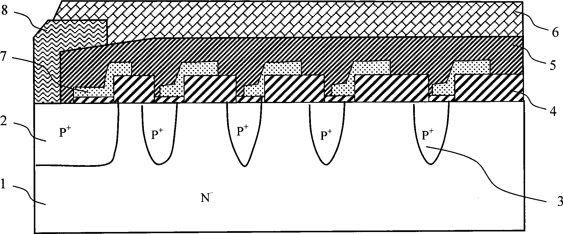
[0028] High voltage power fast recovery diode of the present invention is realized in this way, see Figure 5 As shown, the junction depth of the main junction 2 is 1-3μm, and the doping concentration is 1E16-1E18cm -3 .

[0029] The technical solution matched with this scheme is that the junction terminal is a compound field plate structure, which is composed of a phosphorus-doped polysilicon layer field plate 7 and an aluminum electrode field plate 8, and the aluminum electrode conducts with the phosphorus-doped polysilicon layer, and the aluminum electrode field plate 8 is a multi-level field plate or a stepless gradient field plate, and the dielectric layer 9 is located between the silicon high-resistance layer 1, the phosphorus-doped polysilicon layer field plate 7 and the aluminum electrode field plate 8, see Figure 5 , Figure 6 As shown, the dielectric layer 9 is composed of three parts. From the silicon high resistance layer 1 to the aluminum electrode field plate ...


PUM


Abstract

The invention relates to a high-voltage power-fast-recovery diode and a method for manufacturing the same, which belong to the technical field of semiconductor devices. The forward voltage drop of the prior high-voltage power-fast-recovery diode shows a negative temperature characteristic, thus the thermal reliability is poor. The main junction depth of the high-voltage power-fast-recovery diode is between 1 and 3 microns, and the doping density is between 1E16 and 1E18 cm. A junction terminal is formed by compounding a phosphonium-doped polycrystalline silicon layer field plate and an aluminum electrode field plate, wherein an aluminum electrode is conducted with a phosphonium-doped polycrystalline silicon layer, the aluminum electrode field plate is a multistage field plate or a stepless gradually-changing field plate, and a dielectric layer is positioned between a silicon high-resistance layer and the phosphonium-doped polycrystalline silicon layer and the aluminum electrode field plate. The technological parameters for the manufacturing method to prepare a main junction comprise the following: the temperature is between 1,050 and 1,150 DEG C, the junction pushing time is between 60 and 300 minutes, and the injection dosage is controlled to be between 1*10 and 5*10 cm. The dielectric layer is manufactured on the silicon high-resistance layer provided with the main junction, and the main junction is exposed; a part close to the main junction on the dielectric layer is manufactured with the phosphonium-doped polycrystalline silicon layer field plate at the position close to the main junction; and finally the aluminum electrode field plate is manufactured, and the aluminum electrode field plate is conducted with the main junction and the phosphonium-doped polycrystalline silicon layer field plate and covers part of the dielectric layer.

Description

technical field [0001] The invention relates to a high-voltage power fast recovery diode and a manufacturing method thereof, in particular to a high-current application diode with high thermal reliability requirements, which is applied to the manufacturing field of power fast recovery diodes in discrete and integrated devices, such as The invention relates to chip manufacturing of discrete power fast recovery diodes, manufacturing of power fast recovery diode chips integrated with VDMOS and manufacturing of power fast recovery diode chips integrated with IGBTs, belonging to the technical field of semiconductor devices. Background technique [0002] Power Fast Recovery Diode (hereinafter referred to as FRD—Fast Recovery Diode) is used in power electronic circuits as a freewheeling diode or rectifier and used at the same time as a three-terminal power switching device such as IGBT for switching power supplies, pulse width modulators (PWM) , uninterruptible power supply (UPS), ...

Claims


Application Information

Patent Timeline
Patent Type & Authority Applications(China)
IPC IPC(8): H01L29/861H01L29/36H01L21/22H01L21/324
CPCY02P70/50
Inventor 贾云鹏
Owner JILIN MAGIC SEMICON
Why Eureka
Try Eureka