Method for manufacturing LED chip substrate structure

A technology of light-emitting diode and substrate structure, applied in the direction of electrical components, circuits, semiconductor devices, etc., can solve the problems of photoresist can not reflow convex hull-shaped microstructure, can not manufacture substrates, hinder the luminous efficiency of chips, etc., to reduce the Interfacial reflections, improved defects, reduced absorption loss effects

Active Publication Date: 2010-10-13
EPILIGHT TECH
View PDF3 Cites 0 Cited by
  • Summary
  • Abstract
  • Description
  • Claims
  • Application Information

AI Technical Summary

Problems solved by technology

[0004] However, when preparing the substrate, since the bond energy of the substrate material sapphire has a certain influence on the photoresist, the photoresist often cannot reflow out of the ideal convex-hull microstructure, resulting in the inability to produce an excellent microstructure. Graphical substrate, which hinders the improvement of chip luminous efficiency

Method used


Image

  • Method for manufacturing LED chip substrate structure
  • Method for manufacturing LED chip substrate structure
  • Method for manufacturing LED chip substrate structure

Examples


Embodiment 1

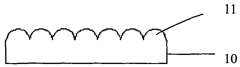
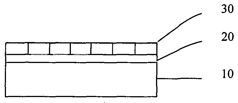
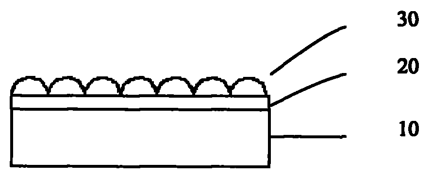
[0027] First refer to Figure 1a As shown, a metal layer 20 is deposited on the sapphire substrate 10 by using an electron beam evaporation machine, the material of the metal layer 20 is titanium, and the thickness is 0.1 nm. Apply photoresist on the metal layer 20 to form a photoresist layer 30, the thickness of the photoresist layer 30 is 0.5um such as Figure 1b shown. Then, the photoresist is patterned on the substrate by a photolithography process to form a desired pattern such as Figure 1c As shown, the pattern is a periodic regular arrangement of cones. Then, the photoresist film layer 30 is reflowed on the metal layer 20 by platform baking photoresist reflow technology, and the photoresist pattern is formed similar to Figure 1d Multiple convex-hull microstructure patterns are shown. The reflux condition is as follows: the baking temperature is 50° C., and the baking time is 0.1 minute. This pattern is then transferred to sapphire using ICP (Inductively Coupled P...

Embodiment 2

[0030] First refer to Figure 1a As shown, a metal layer 20 is plated on the sapphire substrate 10 by using an electron beam evaporation machine, the material of the metal layer 20 is nickel, and the thickness is 20nm. Coat photoresist on this metal layer 20, form one deck photoresist film layer 30, the thickness of photoresist film layer 30 is 2um such as Figure 1b shown. Then, the photoresist is patterned on the substrate by a photolithography process to form a desired pattern such as Figure 1c As shown, the pattern is a periodic regular arrangement of quadrangular prisms. Then, the photoresist film layer 30 is reflowed on the metal layer 20 by platform baking photoresist reflow technology, and the photoresist pattern is formed similar to Figure 1d Multiple convex-hull microstructure patterns are shown. The reflow conditions are as follows: the baking temperature is 200° C., and the baking time is 20 minutes. This pattern is then transferred to sapphire using ICP (In...

Embodiment 3

[0033] First refer to Figure 1a As shown, a metal layer 20 is deposited on a sapphire substrate 10 by using an electron beam evaporation machine, the material of the metal layer 20 is aluminum, and the thickness is 50nm. Coat photoresist on this metal layer 20, form one deck photoresist film layer 30, the thickness of photoresist film layer 30 is 4um such as Figure 1b shown. Then, the photoresist is patterned on the substrate by a photolithography process to form a desired pattern such as Figure 1c As shown, the pattern is a non-periodic regular arrangement of circular frustums. Then, the photoresist film layer 30 is reflowed on the metal layer 20 by platform baking photoresist reflow technology, and the photoresist pattern is formed similar to Figure 1d Multiple convex-hull microstructure patterns are shown. The reflow conditions are as follows: the baking temperature is 400° C., and the baking time is 60 minutes. This pattern is then transferred to sapphire using IC...


PUM

PropertyMeasurementUnit
thicknessaaaaaaaaaa

Abstract

The invention relates to a method for manufacturing an LED chip substrate structure, comprising the following steps: plating a layer of metal layer on the surface of a sapphire substrate, forming a layer of photoresist film layer on the metal layer, patterning the photoresist film layer using the photoetching technology to form the desirable patterns, melting the photoresist film layer using the reflux technology to form a plurality of convex hulls; and transmiting the profiles of the convex hulls on the substrate using the inductively coupled plasma etching process to form convex-hull microstructures on the substrate. By plating a layer of metal on the substrate, the influence from the bond energy of the sapphire substrate to the photoresist can be isolated, therefore, the photoresist iscapable of refluxing more ideal patterns on the surface of the metal layer to help make good-quality substrates with microstructural patterns, reduce the internal absorption and boundary reflection of the LED chips, improve the defect of epitaxial growth, and increase the luminous efficiency of chips.

Description

technical field [0001] The invention relates to a method for manufacturing a substrate structure of a light-emitting diode chip, in particular to a method for manufacturing a substrate structure for improving chip luminous efficiency. Background technique [0002] Light-emitting diodes have the advantages of small size, high efficiency and long life, and are widely used in traffic indication, outdoor full-color display and other fields. In particular, the use of high-power light-emitting diodes may realize semiconductor solid-state lighting, causing a revolution in the history of human lighting, thus It has gradually become a research hotspot in the field of electronics. In order to obtain high-brightness LEDs, the key is to improve the internal quantum efficiency and external quantum efficiency of the device. At present, the light extraction efficiency of the chip is the main factor limiting the external quantum efficiency of the device. The main reason is The refractive in...

Claims


Application Information

Patent Timeline
Patent Type & Authority Patents(China)
IPC IPC(8): H01L33/00
Inventor 袁根如郝茂盛颜建锋李士涛陈诚董云飞
Owner EPILIGHT TECH
Why Eureka
Try Eureka