Manufacturing method for light-emitting diode chip substrate structure

A light-emitting diode and substrate structure technology, which is applied in the direction of electrical components, circuits, semiconductor devices, etc., can solve the problems of poor resistance to reactive ion etching of photoresist, inability to manufacture microstructure pattern substrates, and ineffective photoresist transfer and other issues, to improve the anti-dry etching ability, improve the defects, and reduce the effect of pollution

Active Publication Date: 2010-08-04
EPILIGHT TECH
View PDF1 Cites 0 Cited by
  • Summary
  • Abstract
  • Description
  • Claims
  • Application Information

AI Technical Summary

Problems solved by technology

When preparing a substrate with a convex microstructure, on the one hand, when the photoresist is reflowed, the bond energy of the substrate material sapphire has a certain influence on the photoresist, so that the photoresist often cannot reflow out of the ideal convex microstructure. On the other hand, conventional photoresist has poor resistance to reactive ion etching. After reactive ion etching, photoresist is easily driven into the substrate, which makes the substrate polluted, and the pattern of photoresist cannot be effectively transferred. to the substrate, so that it is impossible to manufacture an excellent microstructure pattern substrate, which hinders the improvement of chip luminous efficiency

Method used


Image

  • Manufacturing method for light-emitting diode chip substrate structure
  • Manufacturing method for light-emitting diode chip substrate structure
  • Manufacturing method for light-emitting diode chip substrate structure

Examples


Embodiment 1

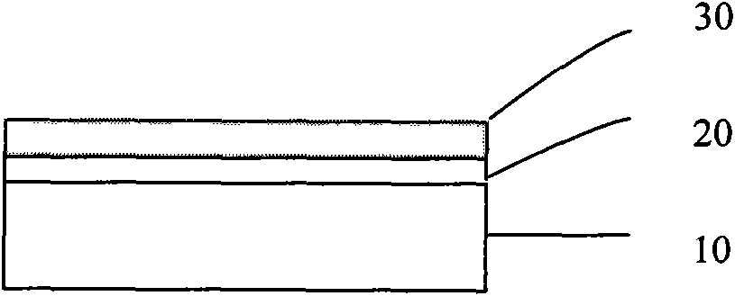
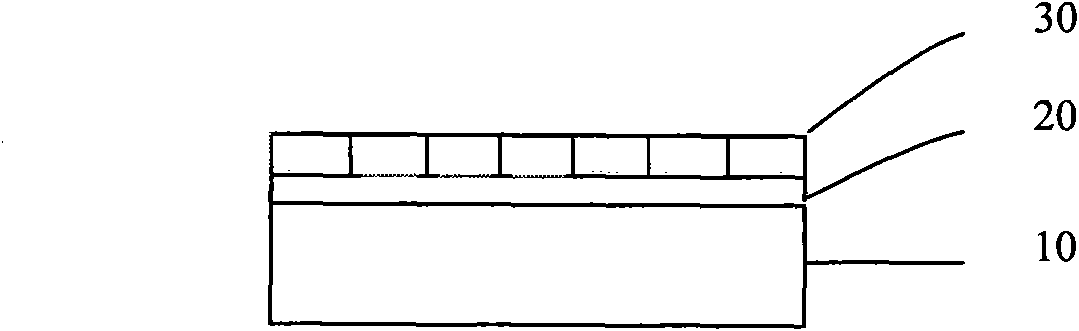
[0037] First refer to Figures 1a-1g The flow chart shown is to prepare the light-emitting diode chip substrate structure. The preparation method of the LED chip substrate structure of the present invention comprises the following steps:

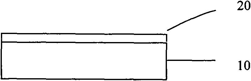
[0038] (1) A metal layer 20 is formed on the surface of the substrate 10 .

[0039] First refer to Figure 1a A metal layer 20 is formed on the surface of the substrate 10 by electron beam evaporation or sputtering technology, wherein the material of the substrate 10 is preferably sapphire. In addition, other conventional electroplating methods can also be used to form the metal layer 20 . The prepared metal layer 20 has a thickness of 1 nm, and its material is titanium. Since a layer of metal layer 20 is placed on the sapphire substrate 10 , the influence of the bond energy of the sapphire substrate 10 on the photoresist can be isolated, and the photoresist can reflow to form a more ideal pattern on the surface of the metal layer 20 .

...

Embodiment 2

[0056] First refer to Figures 1a-1g The flow chart shown is to prepare the light-emitting diode chip substrate structure. The preparation method of the LED chip substrate structure of the present invention comprises the following steps:

[0057] (1) A metal layer 20 is formed on the surface of the substrate 10 .

[0058] First refer to Figure 1a A metal layer 20 is formed on the surface of the substrate 10 by electron beam evaporation or sputtering technology, wherein the material of the substrate 10 is preferably sapphire. In addition, other conventional electroplating methods can also be used to form the metal layer 20 . The prepared metal layer 20 has a thickness of 5 nm, and its material is nickel. Since a layer of metal layer 20 is placed on the sapphire substrate 10 , the influence of the bond energy of the sapphire substrate 10 on the photoresist can be isolated, and the photoresist can reflow to form a more ideal pattern on the surface of the metal layer 20 .

[...

Embodiment 3

[0075] First refer to Figures 1a-1g The flow chart shown is to prepare the light-emitting diode chip substrate structure. The preparation method of the LED chip substrate structure of the present invention comprises the following steps:

[0076] (1) A metal layer 20 is formed on the surface of the substrate 10 .

[0077] First refer to Figure 1a A metal layer 20 is formed on the surface of the substrate 10 by electron beam evaporation or sputtering technology, wherein the material of the substrate 10 is preferably sapphire. In addition, other conventional electroplating methods can also be used to form the metal layer 20 . The prepared metal layer 20 has a thickness of 50 nm, and its material is aluminum. Since a layer of metal layer 20 is placed on the sapphire substrate 10 , the influence of the bond energy of the sapphire substrate 10 on the photoresist can be isolated, and the photoresist can reflow to form a more ideal pattern on the surface of the metal layer 20 . ...


PUM


Abstract

The invention provides a manufacturing method for a light-emitting diode chip substrate structure, which comprises the following steps of: forming a metal layer on the surface of a substrate; forming a photoresist film layer on the obtained metal layer; back washing the obtained photoresist film layer by utilizing the backwash technology; irradiating the photoresist film layer by utilizing deep ultraviolet; causing the obtained photoresist film layer to back wash and volatilize the solvent in the photoresist film layer completely by utilizing the backwash technology; and transferring a patternon the photoresist film layer to a substrate by etching so as to form a plurality of convex microstructures on the surface of the substrate. The method can manufacture the substrate structure with good microstructure, thus reducing boundary reflection and internal absorption of the light-emitting diode chip, improving the defect of epitaxial growth and improing the chip luminous efficiency.

Description

technical field [0001] The invention relates to a method for preparing a substrate structure of a light-emitting diode chip, in particular to a method for preparing a substrate structure for improving chip luminous efficiency. Background technique [0002] Light-emitting diodes have the advantages of small size, high efficiency and long life, and are widely used in traffic indication, outdoor full-color display and other fields. In particular, the use of high-power light-emitting diodes may realize semiconductor solid-state lighting, causing a revolution in the history of human lighting, thus It has gradually become a research hotspot in the field of electronics. In order to obtain high-brightness LEDs, the key is to improve the internal quantum efficiency and external quantum efficiency of the device. At present, the light extraction efficiency of the chip is the main factor limiting the external quantum efficiency of the device. The main reason is The refractive index diff...

Claims


Application Information

Patent Timeline
Patent Type & Authority Patents(China)
IPC IPC(8): H01L33/00
Inventor 袁根如郝茂盛
Owner EPILIGHT TECH
Why Eureka
Try Eureka