High-speed photoelectric subassembly and flip chip structure thereof

A technology for optoelectronic components and electronic chips, applied in electrical components, electro-solid devices, circuits, etc., can solve the problems of difficult to achieve product reliability indicators, difficult to adapt to higher speed requirements, difficult to effectively connect optical and electrical signals, etc. Achieve the effect of reducing the difficulty of development and production and the production cost of products, solving bottleneck problems, and effectively delivering

Active Publication Date: 2009-09-02
WUHAN TELECOMM DEVICES
View PDF0 Cites 51 Cited by
  • Summary
  • Abstract
  • Description
  • Claims
  • Application Information

AI Technical Summary

Problems solved by technology

In the current application of 10G rate devices, the influence of the optical coupling instability of the original technology has already begun to exist, which makes the product reliability index difficult to achieve, the product yield is low, the production time is too long, and the high cost
Obviously, this effect will intensify as the rate increases further
[0013] The above content shows that with the further increase in the speed requirements of optoelectronic devices for communication, some of the original device electrical packaging and optical coupling packaging technologies have begun to be difficult to adapt to higher speed requirements, or in the current technology, to achieve higher speed The effective connection of optical and electrical signals has become more and more difficult, so the author of the present invention has finally obtained this creation through long-term research and practice.

Method used


Image

  • High-speed photoelectric subassembly and flip chip structure thereof
  • High-speed photoelectric subassembly and flip chip structure thereof
  • High-speed photoelectric subassembly and flip chip structure thereof

Examples


Embodiment Construction

[0058] The above and other technical features and advantages of the present invention will be described in more detail below in conjunction with the accompanying drawings.

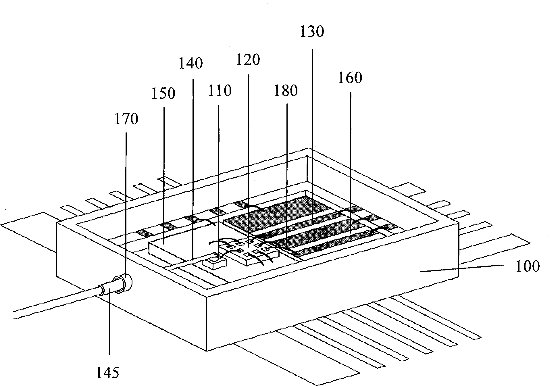
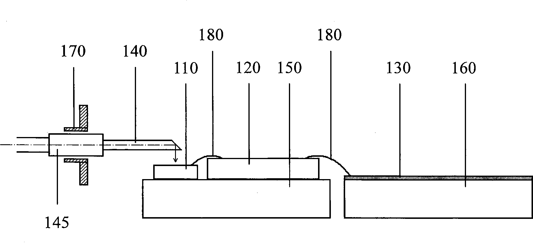
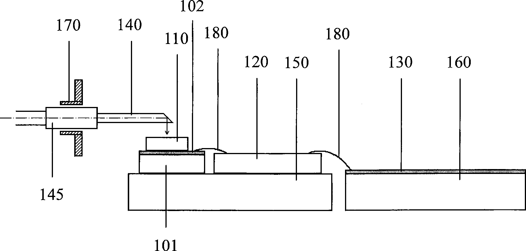
[0059] see Figure 4A and Figure 4B As shown, they are respectively the plane basic structure schematic diagram and the side basic structure schematic diagram of the chip flip chip structure of the present invention. The chip flip chip structure 200 includes: an insulating substrate 210; a photoelectric conversion chip 220, the flip chip surface of which passes through at least A pad 240a is connected to the insulating substrate 210; at least one associated electronic chip 230, whose flip-chip surface is connected to the insulating substrate 210 through at least one pad 240b, and connected to the photoelectric conversion chip 220 A high-speed transmission circuit 240c is provided between them; a high-speed transmission circuit 240d is provided between the associated electronic chip 230 and the high-speed...


PUM


Abstract

The invention relates to a high-speed photoelectric subassembly and a flip chip structure thereof. The flip chip structure comprises an insulating substrate, a photoelectric conversion chip and at least one correlative electronic chip, wherein a flip surface of the photoelectric conversion chip is connected with the insulating substrate through at least one pad; a flip surface of the correlative electronic chip is connected with the insulating substrate through at least one pad; a high-speed transmission circuit is arranged between the correlative electronic chip and the photoelectric conversion chip; another high-speed transmission circuit is arranged between the correlative electronic chip and a high-speed electric signal port of a packaging apparatus; a periphery circuit of a chip is arranged among the photoelectric conversion chip, a correlative electric chip and other parts of the packaging apparatus; and the pads, the high-speed transmission circuits and the periphery circuit of the chip form a metal film circuit on the insulating substrate.

Description

technical field [0001] The invention relates to an improvement of the structure of an optoelectronic device for optical communication, in particular to a novel chip flip-chip structure applied in the field of high-speed optical communication and a corresponding high-speed optoelectronic component. Background technique [0002] In modern life, with the continuous growth of communication traffic, as the main carrier of trunk road information transmission and processing, the optical fiber communication system can solve the problem of capacity expansion and growth. In addition to adding new optical cable lines, an economical solution is The information transmission and processing speed of the original optical fiber line is improved. With the number of communication channels unchanged, this increase in speed requires the related equipment involved in the optical fiber communication system to use optoelectronic devices that can work at a higher rate, including light-emitting devic...

Claims


Application Information

Patent Timeline
Patent Type & Authority Applications(China)
IPC IPC(8): H01L25/00H01L25/16H01L23/52H01L23/48H01L23/12G02B6/42
CPCH01L2224/48091H01L2224/16225H01L2224/48137H01L2224/45144H01L2924/30107H01L2924/3011H01L2224/49109H01L2924/00014H01L2924/00
Inventor 周丹
Owner WUHAN TELECOMM DEVICES
Why Eureka
Try Eureka