
Test vector generating method for boundary scanning

A technology of boundary scan testing and test vectors, applied in the direction of measuring electricity, measuring devices, measuring electrical variables, etc.

Inactive Publication Date: 2009-09-09
MITAC COMP (SHUN DE) LTD
View PDF0 Cites 15 Cited by
  • Summary
  • Abstract
  • Description
  • Claims
  • Application Information

AI Technical Summary

Problems solved by technology

[0005] The purpose of the present invention is to propose a method for generating test vectors that is convenient for generating test vectors and extracting information required for diagnosis, and a relatively complete detection of boundary scan test vectors, which solves the problems of vector generation and diagnostic information extraction in boundary scan

Method used


Image

  • Test vector generating method for boundary scanning

Examples


Embodiment Construction

[0015] Embodiments of the present invention will be described in detail below in conjunction with the accompanying drawings.

[0016] Method of the present invention is to utilize the BSDL (Boundary-Scan Description Language) file of the chip that supports JTAG (Joint Text Action Group) standard and the .NET file (for example: Board Netlist file) of circuit board to generate the .NET file that can be used for JTAG boundary scan failure detection Test vector files and diagnostic information files.

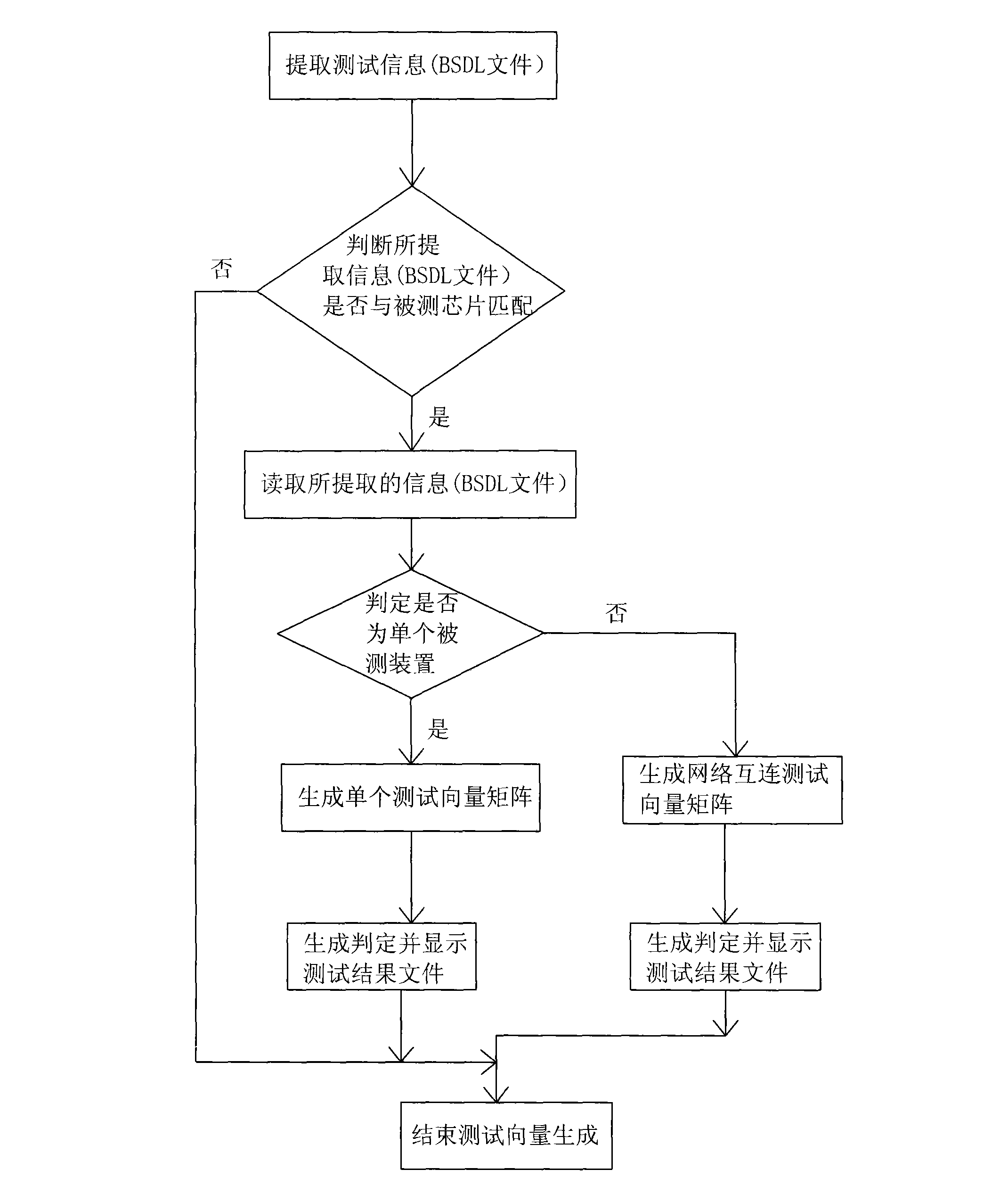
[0017] figure 1 It is a schematic flow chart of the method of the present invention, as shown in the figure, a method for generating a boundary scan test vector, which generates a test vector by integrating test information of a device under test (chip);

[0018] Specific steps are as follows:

[0019] a. Extract test information; extract the relevant information in the BSDL file of each chip provided by the user and the .NET file of the circuit board;

[0020] a1. following step...


PUM


Abstract

The invention discloses a test vector generating method for boundary scanning, which generates a test vector by integrating test information of a tested device. The method comprises the following specific steps: a, extracting the test information; and b, analyzing the test information, and generating a test vector matrix, wherein the vector matrix can be a single test vector matrix and a network interconnecting test vector matrix, and can perform self test and internet test of a single device respectively. The method generates the test vector by integrating the test information of the tested device; the method can conveniently generate the test vector and extract the information required by diagnosis; and simultaneously, the generated test vector is favorable for complete detection and more convenient operation.

Description

technical field [0001] The invention relates to a method for generating test vectors, in particular to a method for generating boundary scan test vectors. Background technique [0002] The detection of faults on the circuit board is usually carried out by using traditional detection equipment such as probes and needle beds. With the development of integrated circuits into the era of VLSI, the high complexity of circuit boards and multi-layer printed boards, surface mount (SMT), ball grid array (BGA), wafer scale integration (WSI) and multi-chip modules The application of (MCM) technology in the circuit system makes the physical accessibility of circuit nodes gradually weakened or even disappears, and the testability of circuits and systems drops sharply. Due to the increasing integration of the circuit board, the distance between the nodes available for testing is getting smaller and smaller, and some even completely become recessive nodes. There are many disadvantages in ...

Claims


Application Information

Patent Timeline
Patent Type & Authority Applications(China)
IPC IPC(8): G01R31/28G01R31/3183G01R31/3185
Inventor 刘占锋
Owner MITAC COMP (SHUN DE) LTD
Learn More