Multi image storage on sensor

An image sensor and charge storage technology, which is applied in the field of sensors and CMOS image sensors, can solve the problems that the combination cannot be completed in a linear manner, and the images can be directly added to achieve the effect of expanding automatic focus, eliminating motion blur, and expanding dynamic range

Inactive Publication Date: 2009-09-16
EASTMAN KODAK CO
View PDF13 Cites 4 Cited by
  • Summary
  • Abstract
  • Description
  • Claims
  • Application Information

AI Technical Summary

Problems solved by technology

However, in the digital case, after these differently illuminated images have been digitally captured and reproduced, combining them using image processing software cannot be done in a linear fashion for the reasons mentioned above
Also, as mentioned above, it is not possible to add the images directly on the sensor due to noise considerations

Method used


Image

  • Multi image storage on sensor
  • Multi image storage on sensor
  • Multi image storage on sensor

Examples


Embodiment Construction

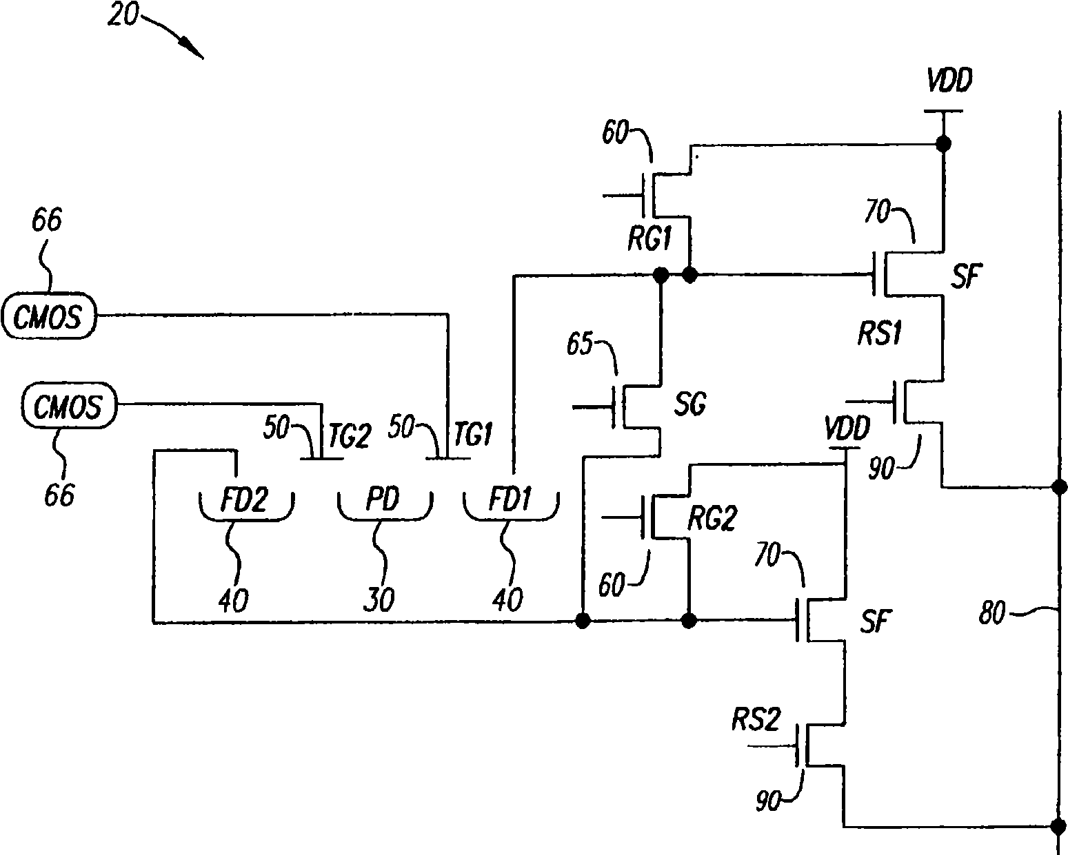
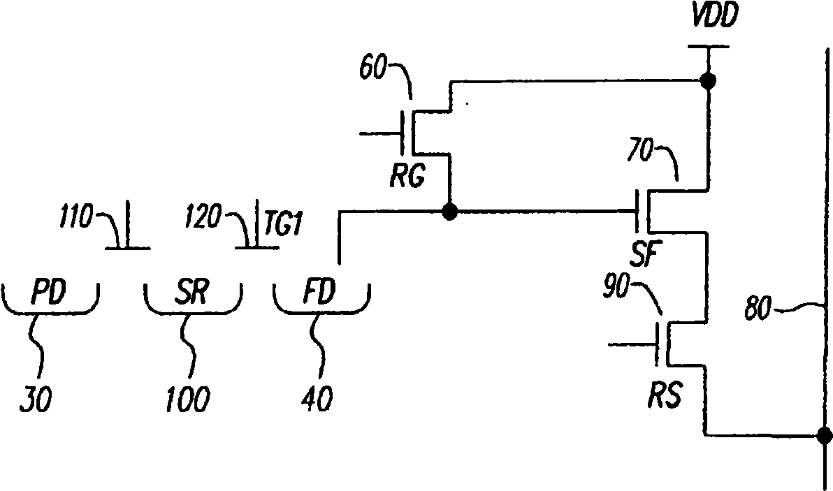
[0032] Before discussing the invention in detail, it is useful to note that the invention is preferably applied to, but is not limited to, CMOS active pixel sensors. Active pixel sensors refer to the active electrical components within the pixels, more specifically amplifiers. CMOS refers to complementary metal-oxide-silicon-type electrical components, such as transistors associated with, but usually not in, a pixel, when the source / drain of the transistor is of one dopant type and its paired transistor is of the opposite dopant type forming the transistor. CMOS devices include the advantage that they consume less energy power.

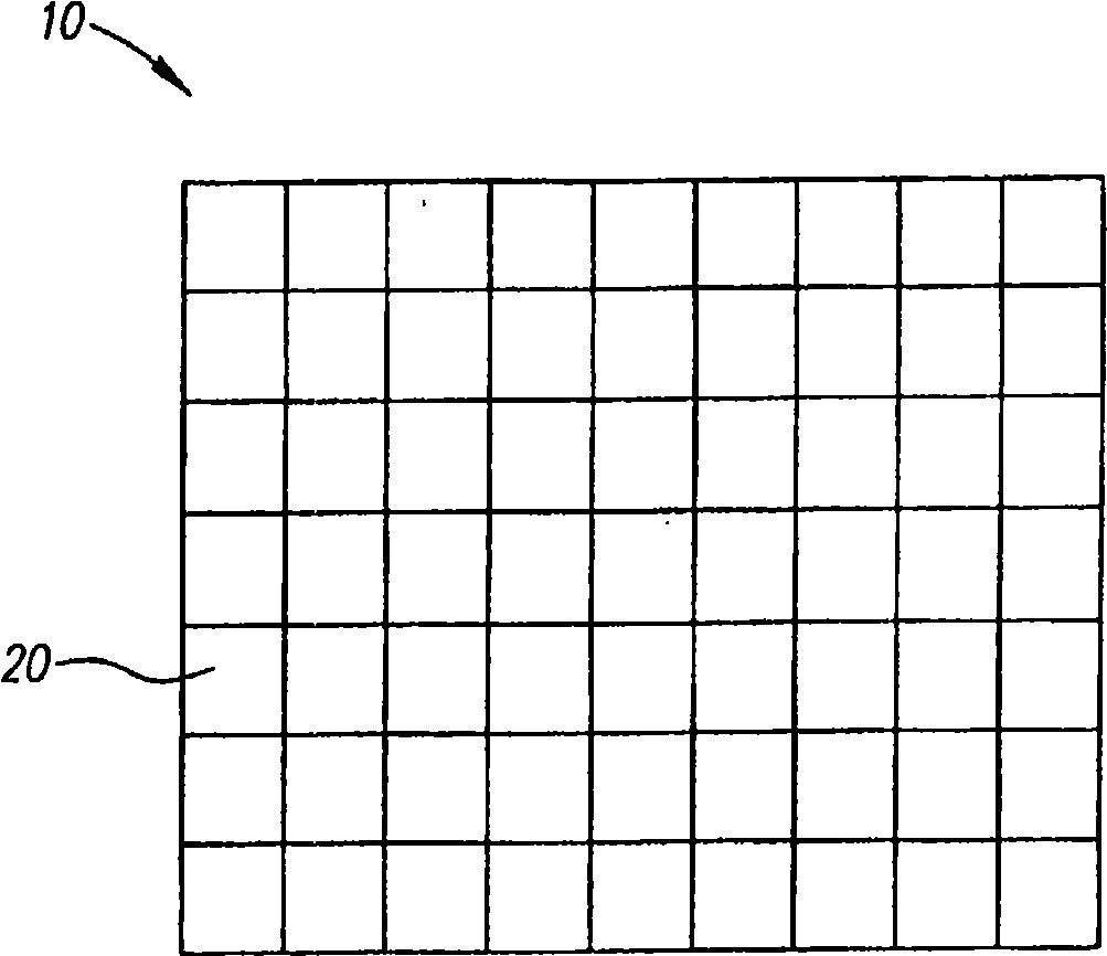
[0033] refer to figure 1 , shows an image sensor 10 of the present invention having a plurality of pixels 20 arranged in a two-dimensional array. As will be apparent to those skilled in the art, although a two dimensional array is shown as a preferred embodiment, the invention is not limited to two dimensional arrays and one dimensional arrays may...


PUM


Abstract

An image sensor includes a plurality of pixels with each pixel having a photosensitive area that captures a sequence of at least two light exposures by accumulating photon-induced charge for each exposure; at least two charge storage areas each of which is associated respectively with one of the sequence of light exposures into which the accumulated charge for each exposure is transferred sequentially; and at least one amplifier that is associated with at least one of the charge storage areas.

Description

technical field [0001] The present invention relates generally to the field of CMOS image sensors, and more particularly to such sensors that capture a sequence of images in two or more floating diffusions respectively. Background technique [0002] Solid state image sensors are now widely used in many types of image capture applications. The two main image sensor technologies employed are Charge Coupled Devices (CCD) and Complementary Metal Oxide Semiconductor (CMOS) devices. Both are basically groups or arrays of photodetectors that convert incident light into electrical signals that can be read out and used to construct an image associated with that incident light pattern. The exposure or integration time of the photodetector array can be controlled by known mechanisms such as mechanical or electronic shutters. The electrical signal represents the amount of light incident on each photodetector in the photodetector array on the image sensor. [0003] Image sensor device...

Claims


Application Information

Patent Timeline
Patent Type & Authority Applications(China)
IPC IPC(8): H04N3/15
CPCH04N5/3745H04N5/3559H04N5/35572H04N5/37452H04N5/35581H04N25/587H04N25/589H04N25/59H04N25/77H04N25/771H04N25/62H04N25/76
Inventor J·N·博尔德J·F·小哈米尔顿J·T·坎普顿
Owner EASTMAN KODAK CO
Why Eureka
Try Eureka