
Method and device for disassembling electronic components from waste printed circuit boards and recovering soldering tin

A technology for waste printed circuit boards and electronic components, which is applied in the field of dismantling of waste printed circuit boards and electronic components and recycling of solder, which can solve the problems of complex components, poor operation effect, difficult recovery of precious metals, etc. Circulation, quality assurance, and low energy consumption

Inactive Publication Date: 2009-09-23
HUNAN VARY TECH
View PDF0 Cites 40 Cited by
  • Summary
  • Abstract
  • Description
  • Claims
  • Application Information

AI Technical Summary

Problems solved by technology

This method has higher crushing benefits in the early stage, but the operability of recycling in the later stage is not high. For example, after the components are crushed together with ceramics and fibers, the components in the product are very complex, and the rich precious metals (gold) are difficult to recycle.
[0006] 3. Make a special fixture to fix the circuit board. After heating, use methods such as beating and eradicating to separate components and solder. This method requires high precision for special fixtures and beating equipment, and there are many types of circuit boards. The operation effect is not good, and it cannot meet the requirements of large-scale processing

Method used


Image

  • Method and device for disassembling electronic components from waste printed circuit boards and recovering soldering tin
  • Method and device for disassembling electronic components from waste printed circuit boards and recovering soldering tin

Examples


Embodiment Construction

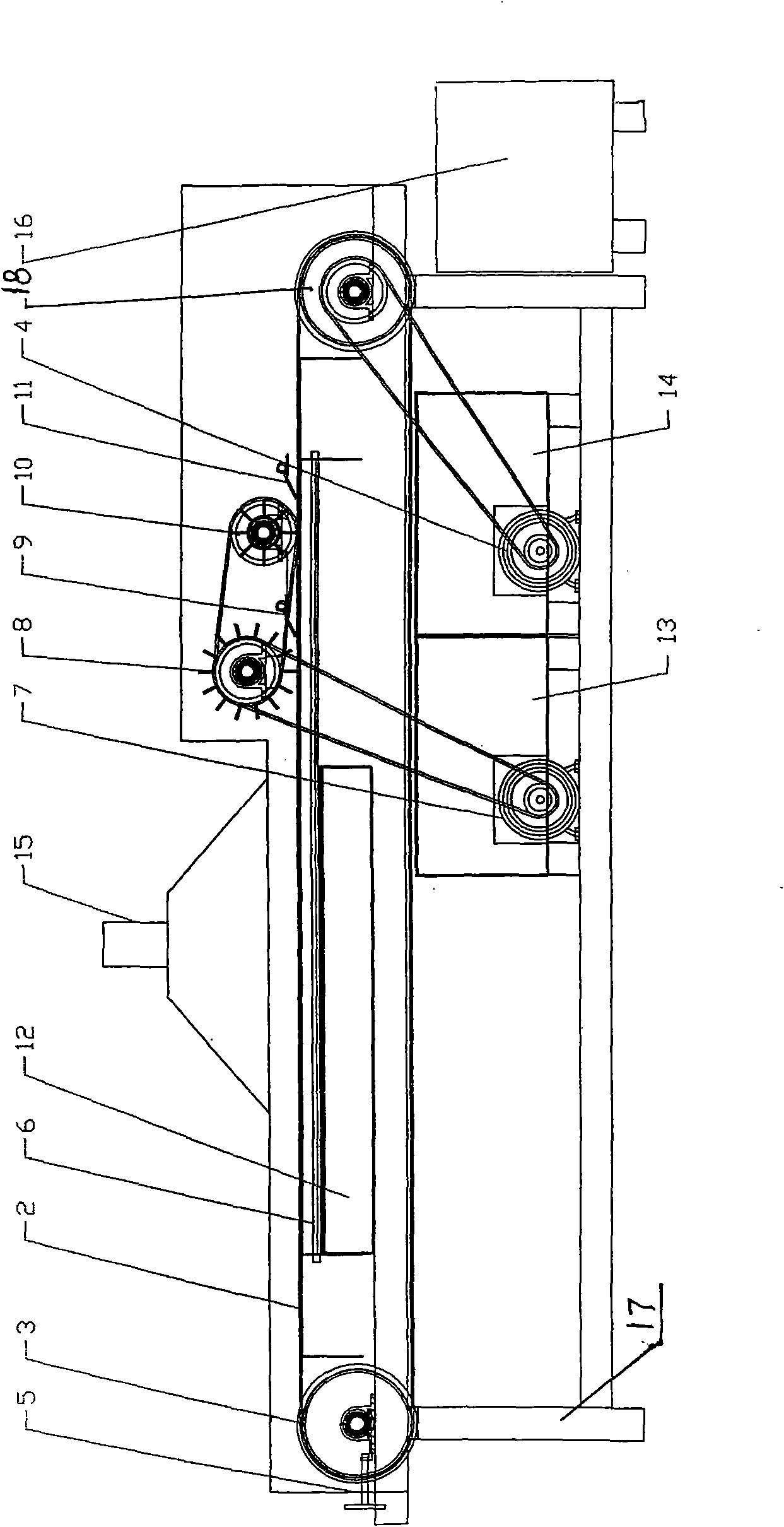
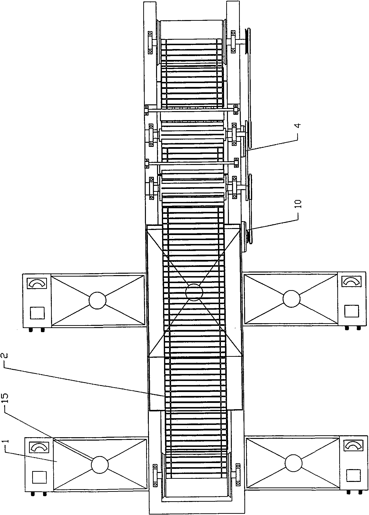
[0026] Referring to the accompanying drawings, the dismantling and solder recovery method of this waste printed circuit board electronic components of the present invention is: place the circuit board with the components face up in the melting tin furnace 1, and the wire leg tin is heated slowly Melt, remove larger components manually, send the circuit board containing small components and solder to the conveyor belt 2 with a self-controlled electric heating device 6 at the bottom, use the hob 8, 10 to suppress the circuit board and move forward For conveying, there are front scraper 9 and rear scraper 11 on the rear side of the hob to shave off components and solder, and through the sequential cooperation of one, two or more sets of hobs and scrapers, the components and solder on the circuit board are separated. The solder is recovered from the receiving basins 12, 13, and 14 under the tin melting furnace and the conveyor belt; the high temperature, peculiar smell, and harmful...


PUM


Abstract

The invention provides a method and a device for disassembling electronic components from waste printed circuit boards (PCB) and recovering soldering tin. The method comprises the following steps: placing the PCB with the electronic components in a temperature-setting tin-melting furnace in a manner that the PCB faces up; grabbing larger electronic components manually and feeding the PCB containing smaller electronic components and soldering tin to the conveyor belt after the soldering tin is melted by heat, wherein, an automatic-control electrical heating and warming device is additionally arranged at the bottom of the conveyor belt; pinning down the PCB by a hob and forwarding the PCB, and eliminating the electronic components and the soldering tin by a scraper arranged on the rear side of the hob, so that the soldering tin can be separated from the electronic components on the PCB through the successive coordinating operation of hobs and scrapers in a plurality of groups; recovering the soldering tin by a material-receiving pot; and subjecting the peculiar smell and harmful gases generated by heating the PCB to negative-pressure air draft and absorption treatment and discharging the gases until the discharge standards are met. The invention is suitable for treating PCBs with various thicknesses and recovering electronic components of various types and models; the invention has the advantages of high speed, high efficiency, no pollution, high operability and advanced technology; and the invention contains a novel and environment-friendly method and an equipment for disassembling the waste printed circuit boards and recovering treatment of soldering tin.

Description

Technical field: [0001] The invention relates to the technical field of environmental protection, in particular to a method and equipment for dismantling electronic components of waste printed circuit boards and recycling solder. Background technique: [0002] With the rapid development of the information industry, the replacement of electronic products is more frequent, and the number of eliminated and scrapped circuit boards is increasing, which has caused a huge impact on the environment and hidden dangers of pollution. At present, landfill, washing, incineration and other methods are generally used to dispose of waste circuit boards. Since the polymeric organic matter is difficult to degrade under natural conditions, toxic and harmful components such as heavy metals enter the biological chain through water, air, and soil, which poses a threat to human health and serious harm to the ecological environment. Therefore, the disposal of discarded circuit boards has become a ...

Claims


Application Information

Patent Timeline
IPC IPC(8): B23K1/018B23K3/08B09B3/00
CPCY02W30/82
Inventor 明果英邓建平张宇平李麒麟林常青
Owner HUNAN VARY TECH
Learn More