
Wavelength division multiplexer/demodulation multiplexer based on multimode interference effect of two-dimensional photonic crystals

A two-dimensional photonic crystal and wavelength division multiplexer technology, which is applied in the directions of light guides, optics, instruments, etc., can solve the problems of unpredictable working frequency and ineffective application, and achieves the improvement of wavelength division multiplexing/demultiplexing efficiency, Compact, easy-to-integrate effects

Inactive Publication Date: 2009-09-30
SOUTHEAST UNIV
View PDF0 Cites 9 Cited by
  • Summary
  • Abstract
  • Description
  • Claims
  • Application Information

AI Technical Summary

Problems solved by technology

Existing devices can only be designed for one operating frequency, and the accompanying other operating frequencies are unpredictable, so they cannot be effectively applied

Method used


Image

  • Wavelength division multiplexer/demodulation multiplexer based on multimode interference effect of two-dimensional photonic crystals
  • Wavelength division multiplexer/demodulation multiplexer based on multimode interference effect of two-dimensional photonic crystals
  • Wavelength division multiplexer/demodulation multiplexer based on multimode interference effect of two-dimensional photonic crystals

Examples


Embodiment Construction

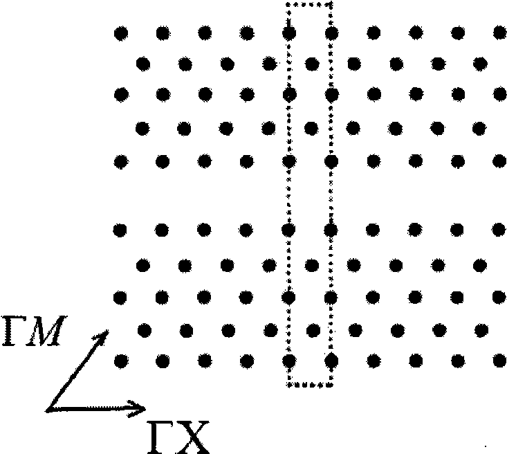
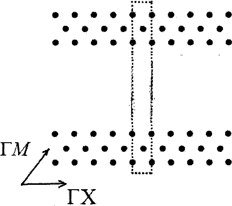
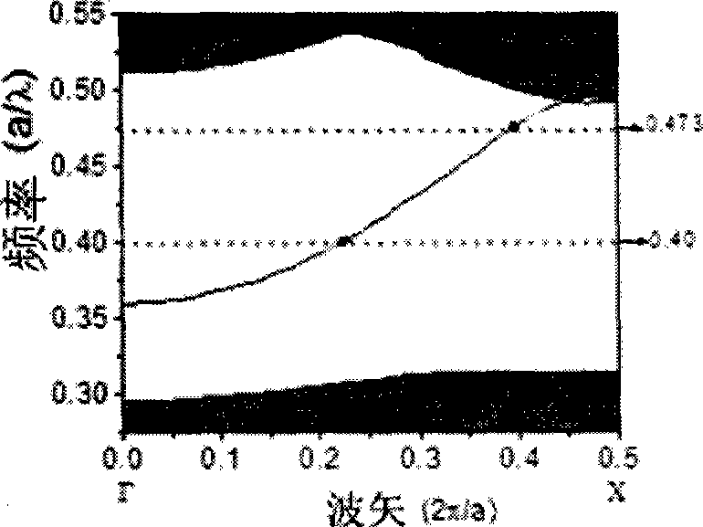
[0027] The invention provides a wavelength division multiplexer / demultiplexer based on the multimode interference effect of two-dimensional photonic crystals, and the implementation includes the following steps:

[0028] 1. Select the material, determine the refractive index of the material, select the photonic crystal lattice type, and determine the ratio of the dielectric column or hole radius to the lattice constant;

[0029] Select Si dielectric pillars with dielectric constant ε=12 to form a two-dimensional triangular lattice structure. The axis of the dielectric pillars is along the z-axis direction, and the radius of the dielectric pillars is r / a=0.16, where a is the lattice constant and is temporarily a parameter. Of course, the photonic crystal can also be composed of air columns, so the following dielectric columns can also be air columns.

[0030] 2. Introduce line defects into photonic crystals to form single-mode waveguides and multi-mode waveguides, and use the p...


PUM


Abstract

The invention provides a wavelength division multiplexer / demultiplexer based on the multimode interference effect of two-dimensional photonic crystals, comprising a monomode waveguide (1), a multimode interference waveguide (2), a monomode waveguide (3) and a monomode waveguide (4), wherein the monomode waveguide (3) and the monomode waveguide (4) are parallel. The invention confirms the length of the multimode waveguide according to the self-imaging conditions of two preset frequency positions so that after light is input from the monomode waveguide (1) in the two frequency positions, light in one frequency position is imaged on the monomode waveguide (3), and light in the other frequency position is imaged on the monomode waveguide (4) so as to realize the function of a wavelength division demultiplexer. Light with a frequency satisfying an imaging condition is respectively input from the monomode waveguide (3) and the monomode waveguide (4) and output from the monomode waveguide (1) so as to realize the function of a wavelength division multiplexer. The invention has the advantages of compact structure, easy integration, and the like and has wide application prospects in future optical communication.

Description

technical field [0001] The invention provides a two-dimensional photonic crystal wavelength division multiplexer / demultiplexer and a design method thereof, and relates to the technical fields of photonic crystals, optical communications, and the like. Background technique [0002] Photonic crystals are artificially constructed new materials with photophysical functions whose refractive index changes periodically. When the electromagnetic wave propagates in it, due to Bragg scattering, the electromagnetic wave will be modulated to form an energy band structure, which is called a photon energy band. There is a band gap between the photonic energy bands, that is, the photonic band gap or the photonic forbidden band. The photonic bandgap is a frequency region in which the frequency of the incident light falls, and the light is totally reflected and cannot pass through the photonic crystal. When a line defect is introduced into a complete photonic crystal, the light in the forb...

Claims


Application Information

Patent Timeline
IPC IPC(8): G02B6/122
Inventor 张家雨张玲玲王琼崔一平
Owner SOUTHEAST UNIV
Learn More