Supercharge Your Innovation With Domain-Expert AI Agents!

Electrical level translation circuit

A technology for converting circuits and levels, applied in the direction of logic circuits, logic circuit connection/interface layout, electrical components, etc., can solve the problems of power consumption, slow level conversion circuit 10, pulling, etc., to achieve the effect of improving the conversion speed

Inactive Publication Date: 2009-09-30
RAYDIUM SEMICON
View PDF0 Cites 6 Cited by
  • Summary
  • Abstract
  • Description
  • Claims
  • Application Information

AI Technical Summary

Problems solved by technology

[0010] In addition, since the transistor N2 and the transistor P2 are both in the conduction state, the output signal OUT will be at the power supply voltage V DD and the power supply voltage Vss pull phenomenon
[0011] In this way, not only the traditional level conversion circuit 10 is too slow, but also the short-circuit current I DS1 It will also cause unnecessary power consumption (PowerConsumption) of the level conversion circuit 10
In addition, when the power supply voltage Vcc is turned off and the power supply voltage VDD is still on, since the output signal OUT and the inverted output signal OUT' are floating, a large leakage current will be induced.

Method used


Image

  • Electrical level translation circuit
  • Electrical level translation circuit
  • Electrical level translation circuit

Examples


Embodiment 1

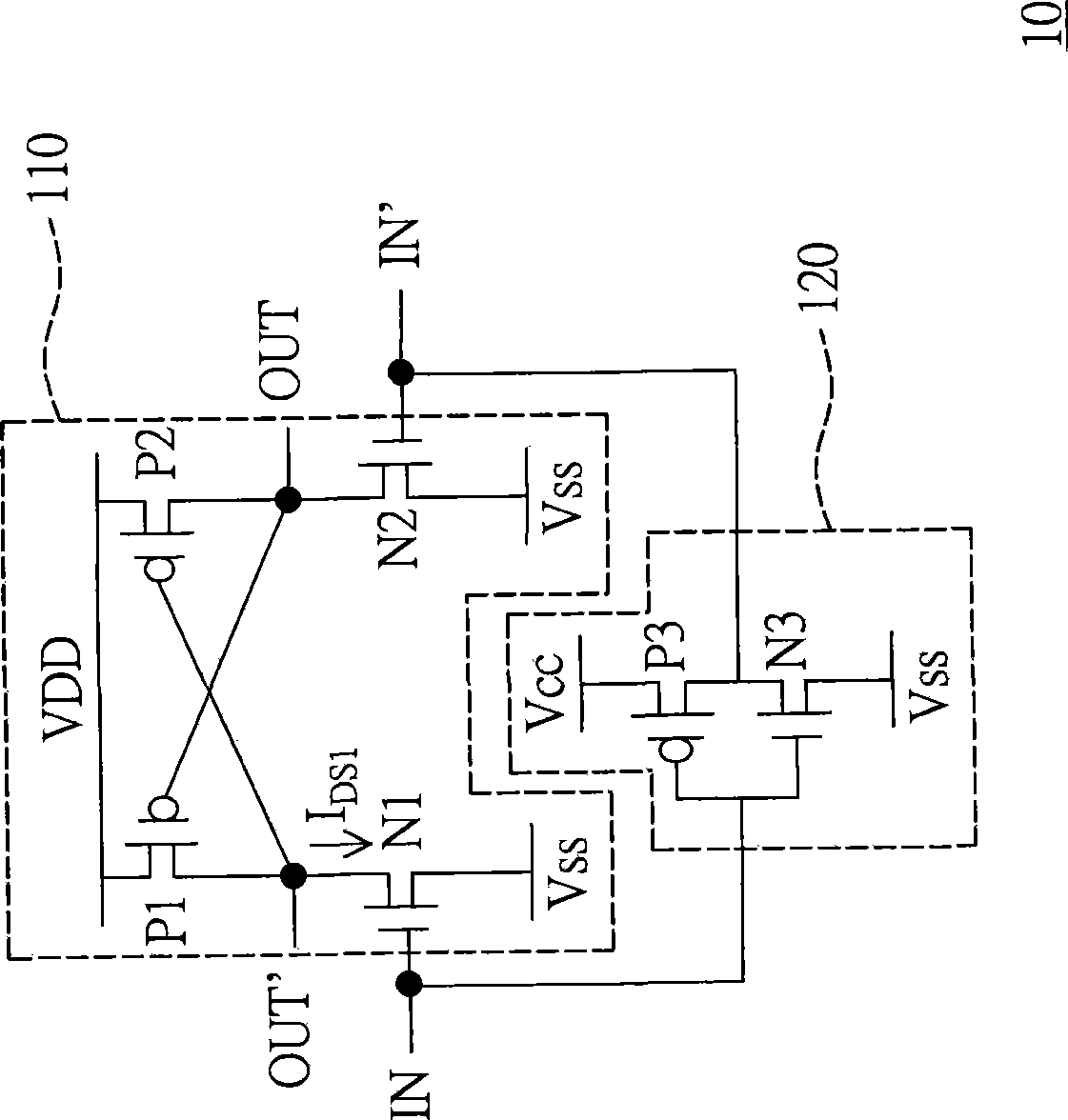
[0056] Please refer to Figure 5 , which shows a circuit diagram of a level conversion circuit according to Embodiment 1 of the present invention. The aforementioned level shifting circuit 40 and inverter 420 are represented by level shifting circuit 50 and inverter 520 respectively in Embodiment 1, and the first switch circuit 430 and the second switch circuit 440 are respectively represented by A first switch circuit 530 and a second switch circuit 540 are shown. For the convenience of description, the following description takes the input signal IN and the inverted input signal IN' between 0-1.8V as an example. In addition, it is illustrated by taking the output signal OUT and the inverted output signal OUT' between 0V and 5V as an example.

[0057] The first switch circuit 530 further includes a transistor N3, and the transistor N3 is, for example, an N-type metal oxide semiconductor transistor. The first terminal of the transistor N3 is coupled to the control terminal ...

Embodiment 2

[0067] Please refer to Figure 8 , which shows a circuit diagram of a level conversion circuit according to Embodiment 2 of the present invention. The aforementioned level conversion circuit 40 and inverter 420 are represented by level conversion circuit 90 and inverter 920 respectively in the second embodiment, and the first switch circuit 430 and the second switch circuit 440 are respectively represented in the second embodiment It is represented by a first switch circuit 930 and a second switch circuit 940 .

[0068] The first switch circuit 930 further includes a transistor N3 and a transistor N4, and the transistor N3 and the transistor N4 are, for example, N-type metal oxide semiconductor transistors. The transistor N3 is connected in series with the transistor N4, and the first terminal of the transistor N3 is coupled to the control terminal of the transistor P2. The second terminal of the transistor N3 is coupled to the first terminal of the transistor N4, and the se...


PUM


Abstract

The invention discloses an electrical level translation circuit, which comprises an electrical level translator, an inverter, a first switch circuit and a second switch circuit. The electrical level translator comprises a first transistor, a second transistor, a third transistor and a fourth transistor. The inverter is used for receiving an input signal and accordingly generates an inverse input signal. The first transistor and the second transistor are controlled by the input signal and an output signal respectively to output an inverse output signal. While the third transistor and the fourth transistor are controlled by the inverse input signal and the inverse output signal respectively to output the output signal. The first switch circuit is coupled to the electrical level translator and turns off the fourth transistor when the third transistor is turned on. While the second switch circuit is coupled to the electrical level translator and turns off the second transistor when the first transistor is turned on.

Description

technical field [0001] The present invention relates to a level shifter circuit, and in particular to a voltage shifter circuit which improves switching speed and reduces short-circuit current. Background technique [0002] Please refer to figure 1 , which shows a circuit diagram of a conventional level shifting circuit. The conventional level shifting circuit 10 includes a level shifter 110 and an inverter 120 . The inverter 120 is used to receive the input signal IN and invert it to generate an inverted input signal IN' and output it to the level shifter 110 . Wherein, the inverter 120 includes a transistor P3 and a transistor N3, and the transistor P3 and the transistor N3 are respectively a P-type metal-oxide-semiconductor transistor (PMOS) and an N-type metal-oxide-semiconductor transistor (NMOS). The control terminal of the transistor P3 is coupled to the control terminals of the transistor N3 and the transistor N1, and the second terminal of the transistor P3 is co...

Claims


Application Information

Patent Timeline
Patent Type & Authority Applications(China)
IPC IPC(8): H03K19/017H03K19/0185H03K19/003
Inventor 洪根刚李武松
Owner RAYDIUM SEMICON
Features
  • R&D
  • Intellectual Property
  • Life Sciences
  • Materials
  • Tech Scout
  • Unparalleled Data Quality
  • Higher Quality Content
  • 60% Fewer Hallucinations
Learn More