Method for preparing uniform three dimensional nanometer fluid passage by femto-second laser

A femtosecond laser, three-dimensional nanotechnology, applied in nanotechnology, nanotechnology, nanostructure manufacturing and other directions, can solve the problems of low inner wall finish, limited length, complex three-dimensional micro-nano hollow structure, etc., and achieve the effect of high finish

Inactive Publication Date: 2009-10-07
SHANGHAI INST OF OPTICS & FINE MECHANICS CHINESE ACAD OF SCI
View PDF0 Cites 14 Cited by
  • Summary
  • Abstract
  • Description
  • Claims
  • Application Information

AI Technical Summary

Problems solved by technology

[0004] The technical problem to be solved by the present invention is to overcome the disadvantages of poor channel uniformity, low inner wall finish and limited length (only on the order of submillimeters) in the preparation of microfluidic channels by the above-mentioned existing femtosecond laser micromachining technology, and provide a A method for preparing a uniform three-dimensional nanofluidic channel using a femtosecond laser, and further stretching the inner diameter of the channel to the nanometer level, thereby realizing a complex three-dimensional micro-nano hollow structure on a single transparent material chip

Method used


Image

  • Method for preparing uniform three dimensional nanometer fluid passage by femto-second laser
  • Method for preparing uniform three dimensional nanometer fluid passage by femto-second laser
  • Method for preparing uniform three dimensional nanometer fluid passage by femto-second laser

Examples


Embodiment Construction

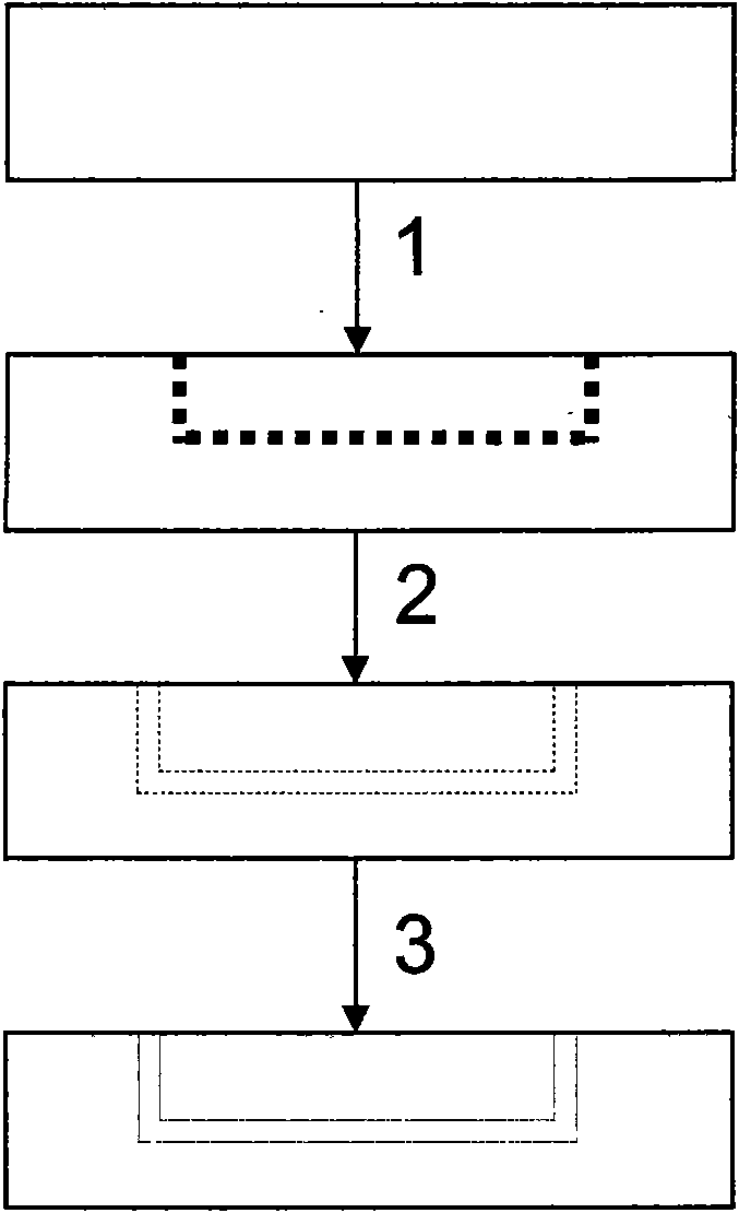
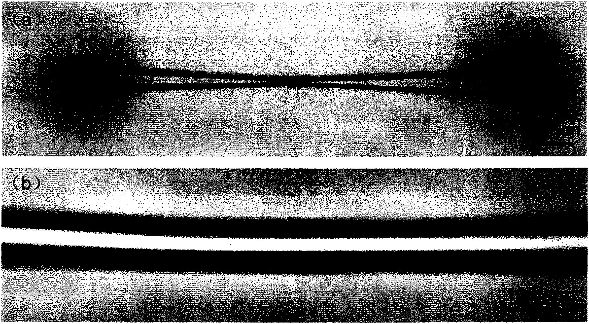
[0021] Below by embodiment the present invention will be further described, but should not limit protection scope of the present invention with this. see first figure 1 , figure 1 It is a schematic flow chart of the method for preparing a uniform three-dimensional nanofluidic channel by using a femtosecond laser in the present invention. Now, taking quartz glass as an example to illustrate the method of the present invention, it can be seen from the figure that the method for preparing a uniform three-dimensional nanofluidic channel by using a femtosecond laser in the present invention includes Follow these three steps:

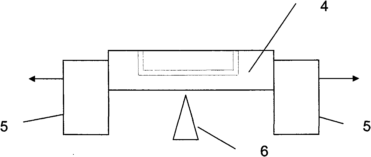
[0022] (1) Femtosecond laser irradiation: Take a quartz glass sample 4 with a size of 10mm×5mm×1mm and polish the upper and lower surfaces, and fix it on a three-dimensional displacement platform after cleaning; when the femtosecond laser directly writes a three-dimensional pattern inside the quartz glass sample 4 The pulse width is 40±2fs, the center wavel...


PUM


Abstract

A method for preparing uniform three dimensional nanometer fluid passage by femto-second laser comprises the steps of irradiating transparent material by femto-second laser, chemical attacking and hot drawing. the three dimensional nanometer fluid passage prepared by the method in the invention achieves the advantages of uniform longitudinal appearance, good roundness of passage cross section, high smoothness of the passage inner wall and small passage inner diameter to nanometer scale.

Description

technical field [0001] The invention relates to femtosecond laser processing, in particular to a method for preparing uniform three-dimensional nanofluid channels by using femtosecond laser. The method is suitable for preparing micro-nano fluid devices inside various transparent materials, crystals, transparent polymers and other materials. Background technique [0002] Micro-total analysis systems and lab-on-a-chip devices try to integrate multiple functional devices such as microfluidics, micro-optics, microelectronics, and micro-mechanics on the same chip that is only the size of a palm. It has traditional biochemical properties such as low consumption, high efficiency and high sensitivity. The incomparable advantages of analytical systems have now set off a major revolution in the fields of biology, chemistry, and medical science. The current mainstream three-dimensional micro-nano device manufacturing technology mainly relies on the method of semiconductor lithography,...

Claims


Application Information

Patent Timeline
Patent Type & Authority Applications(China)
IPC IPC(8): B82B3/00
Inventor 程亚何飞孙海轶徐至展
Owner SHANGHAI INST OF OPTICS & FINE MECHANICS CHINESE ACAD OF SCI
Why Eureka
Try Eureka