Control circuit of cascade type buck-boost converter and control method thereof
A buck-boost converter and control circuit technology, applied in control/regulation systems, conversion of DC power input to DC power output, instruments, etc., can solve problems such as unstable converters, complicated control, and less research, and achieve Achieve simple, high-efficiency conversion effects
- Summary
- Abstract
- Description
- Claims
- Application Information
AI Technical Summary
Problems solved by technology
Method used
Image

Examples
Embodiment Construction
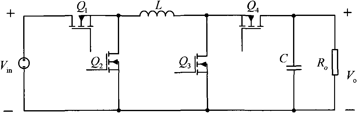
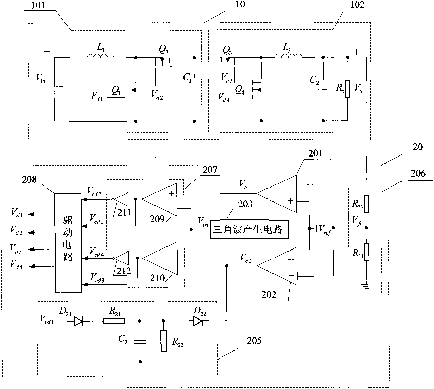
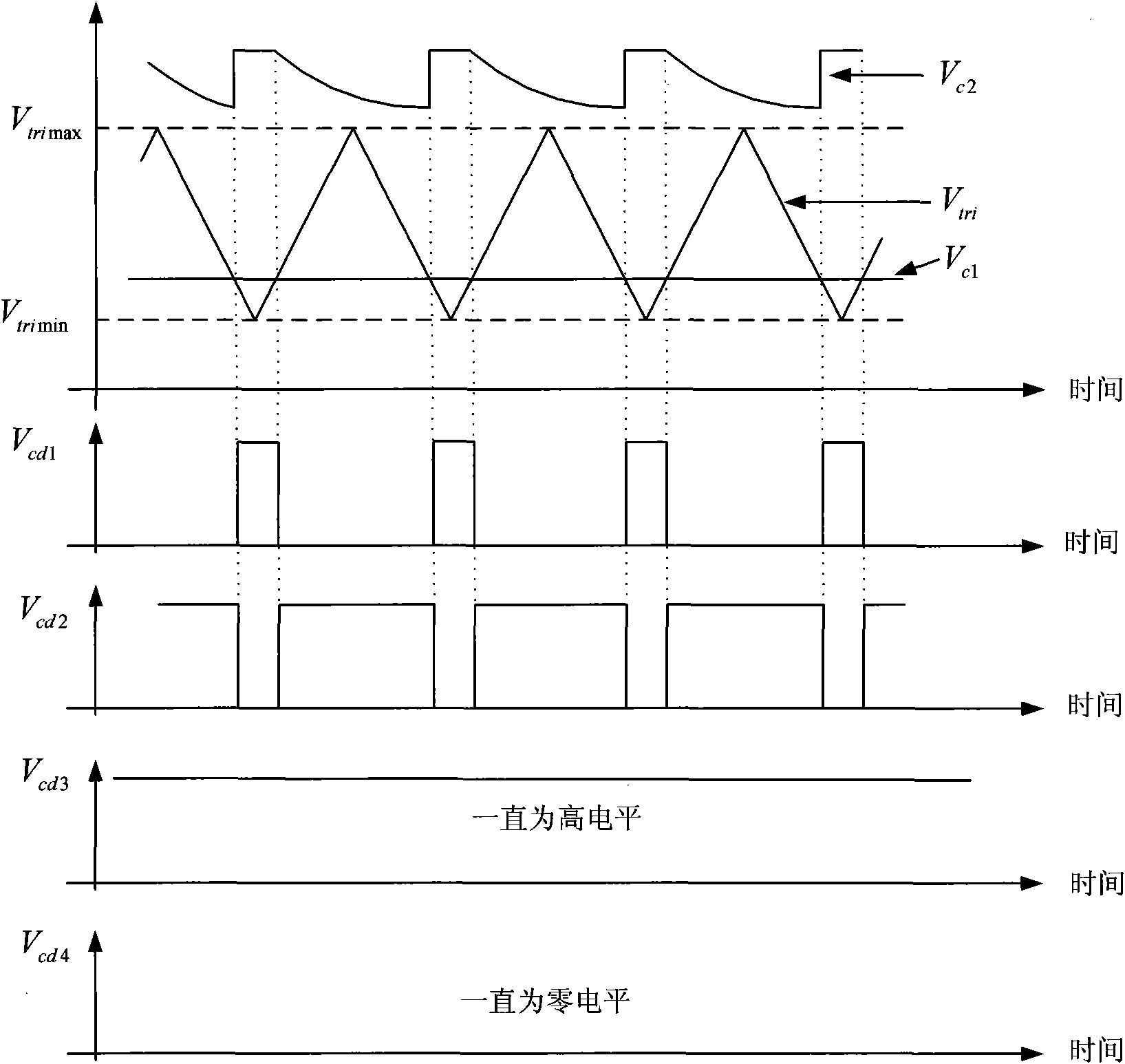
[0017] Such as figure 2 As shown, the schematic diagram of the cascaded buck-boost converter and its control circuit involved in the embodiment of the present invention.
[0018] figure 2 The main circuit topology 10 of the intermediate cascaded buck-boost converter includes a DC power supply V in , four power switch tubes Q 1 , Q 2 , Q 3 and Q 4 , two inductors L 1 and L 2 , two filter capacitors C 1 and C 2 , resistance R o , where: DC power supply V in Positive connection inductance L 1 at one end, the inductance L 1 The other ends are connected to the power switch tube Q 1 The drain and power switch Q 2 source, the power switch Q 2 The drains are respectively connected to the filter capacitor C 1 One end of the power switch tube Q 3 The drain of the power switch tube Q 3 The sources are respectively connected to the inductor L 2 One end of the power switch tube Q 4 the drain, the inductance L 2 The other end is connected to the filter capacitor C 2 ...
PUM
 Abstract
Description
Claims
Application Information