TFT-LCD array substrate structure and manufacturing method thereof

An array substrate structure and thin-film transistor technology, which is applied in semiconductor/solid-state device manufacturing, semiconductor devices, electric solid-state devices, etc., can solve the problems of low jump voltage, small storage capacitance, and affecting the display quality of thin-film transistor liquid crystal displays, etc., to achieve Reduced jump voltage, increased storage capacitance, and improved display quality

Active Publication Date: 2009-10-21
K TRONICS (SUZHOU) TECH CO LTD +1
View PDF0 Cites 9 Cited by
  • Summary
  • Abstract
  • Description
  • Claims
  • Application Information

AI Technical Summary

Problems solved by technology

[0011] In the process of realizing the present invention, the inventors found that there are at least the following problems in the prior art: due to the formation of storage capacitance between the pixel electrode 10 and the gate scanning line 1, the pixel electrode 10 and the common electrode lead 11, such as Figure 1b As shown, there is a two-layer structure of gate insulating layer 4 and passivation layer 8 between the pixel electrode 10 and the gate scanning line 1 (not shown in the figure) and the common electrode lead 11, resulting in the pixel electrode 10 and the gate scanning line 1. The distance between the pixel electrode 10 and the common electrode lead is large, the storage capacitance is small, and the jump voltage is low, which in turn affects the display quality of the thin film transistor liquid crystal display; in addition, the 5-Mask process needs to be carried out in five steps Exposure process, the process cycle is too long, the production efficiency is low, and the production cost is high

Method used


Image

  • TFT-LCD array substrate structure and manufacturing method thereof
  • TFT-LCD array substrate structure and manufacturing method thereof
  • TFT-LCD array substrate structure and manufacturing method thereof

Examples


Embodiment Construction

[0041] The present invention will be described in further detail below in conjunction with the accompanying drawings.

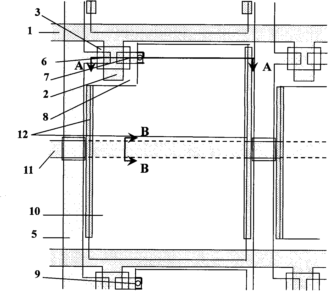
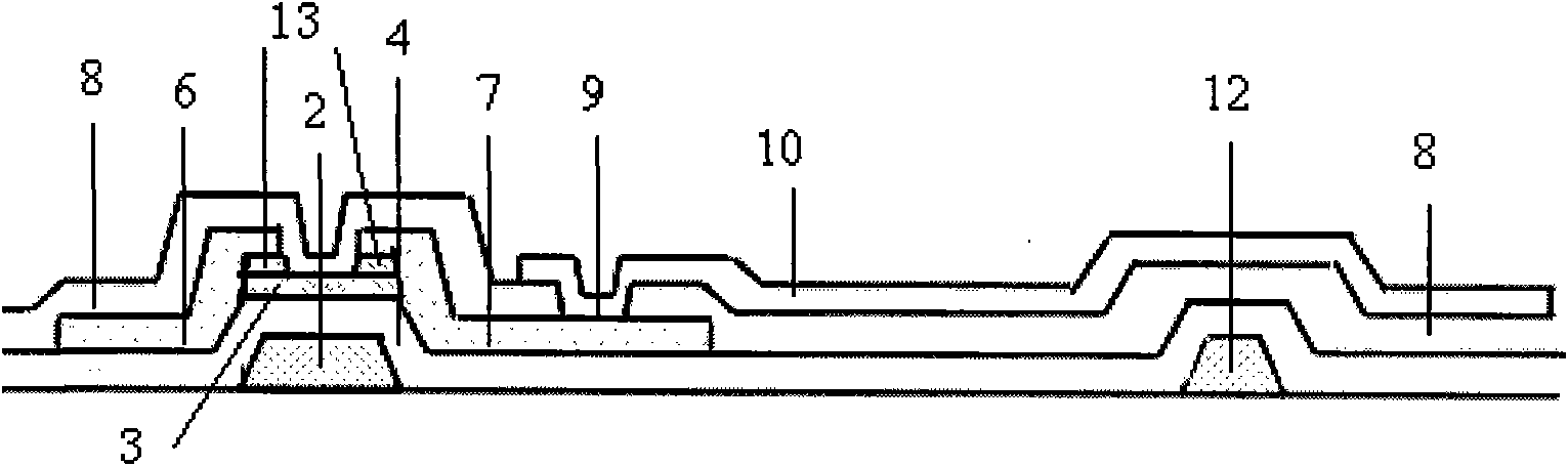
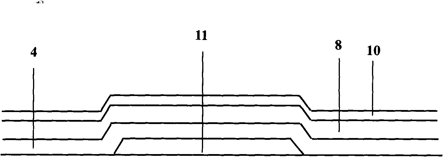
[0042] In order to solve the problem of poor display quality of liquid crystal display panels in the prior art, the present invention provides a thin film transistor liquid crystal display array substrate structure. Such as image 3 , Figure 3a As shown, the array substrate structure includes: gate scanning lines 1 and data scanning lines 5 formed on the substrate, and pixel electrodes 10 are formed in pixel regions defined by adjacent gate scanning lines 1 and data scanning lines 5, And form a thin film transistor at the intersection; the composition structure of the thin film transistor is as follows from bottom to top: gate electrode 2, gate insulating layer 4, transparent conductive layer (not marked in the figure), source electrode 6 and drain electrode 7, Ohmic contact layer 13 , semiconductor layer 3 , passivation layer 8 . The structure of the arr...


PUM


Abstract

The invention discloses a TFT-LCD array substrate structure and a manufacturing method thereof, relates to the technical field of TFT-LCDs and aims at solving a problem of poor display quality of TFT-LCDs in the prior art. The TFT-LCD array substrate structure comprises a grid scanning line and a data scanning line formed on a substrate. A pixel electrode is formed in a pixel area defined by the grid scanning line and the data scanning line which are adjacent, and a TFT is formed at a crossing. The constitutional structure of the TFT comprises a grid electrode, a grid insulating layer, another grid insulating layer, a transparent conducting layer, a source electrode, a drain electrode, an ohmic contact layer, a semiconductor layer and a passivation layer from the bottom up, wherein, a contact part between the transparent conducting layer and the drain electrode is the pixel electrode, and the source electrode is connected with the data scanning line. The TFT-LCD array substrate structure is suitable for improving the display quality of the TFT-LCD.

Description

technical field [0001] The invention relates to the technical field of thin film transistor liquid crystal displays, in particular to a thin film transistor liquid crystal display array substrate structure and a manufacturing method. Background technique [0002] At present, with the development of science and technology, in flat panel display technology, thin film transistor liquid crystal display (TFT-LCD) has become the preferred choice for information display due to its excellent display quality, relatively low manufacturing cost, low power consumption and no radiation. The display quality of mainstream products has also been continuously improved with the progress of manufacturing technology. [0003] TFT-LCD is formed by combining an array substrate and a color filter substrate. At present, the mainstream amorphous silicon TFT-LCD array substrate structure usually adopts a bottom gate structure with back channel etching. Such as figure 1 , Figure 1a As shown, the s...

Claims


Application Information

Patent Timeline
Patent Type & Authority Applications(China)
IPC IPC(8): G02F1/1362H01L27/12H01L21/84
CPCG02F2001/136231G02F2001/136236G02F1/133512G02F1/136236G02F1/136231
Inventor 张弥
Owner K TRONICS (SUZHOU) TECH CO LTD
Why Eureka
Try Eureka