Method for producing ONO structure

A wet etching and oxide film technology, applied in semiconductor/solid-state device manufacturing, electrical components, semiconductor devices, etc., can solve problems such as poor etching uniformity, photoresist peeling, and increase in size, and achieve control of lateral etching. etch, eliminate peeling problems, improve window performance

Inactive Publication Date: 2009-10-28
SHANGHAI HUA HONG NEC ELECTRONICS
View PDF0 Cites 9 Cited by
  • Summary
  • Abstract
  • Description
  • Claims
  • Application Information

AI Technical Summary

Problems solved by technology

[0005] The existing technology uses a photoresist mask when opening the lower oxide film by chemical wet method, and the type and quantity of the treatment solution are very limited. If the treatment time is too long, it will easily cause the problem of photoresist stripping. The etching rate of the oxide film of the chemical solution is too fast and it is easy to cause the problem of poor etching uniformity, especially if the upper oxide film is etched sideways too much, the size will be seriously increased.

Method used


Image

  • Method for producing ONO structure
  • Method for producing ONO structure
  • Method for producing ONO structure

Examples


Embodiment Construction

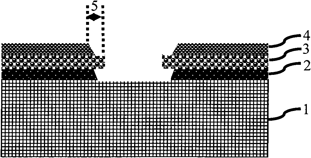
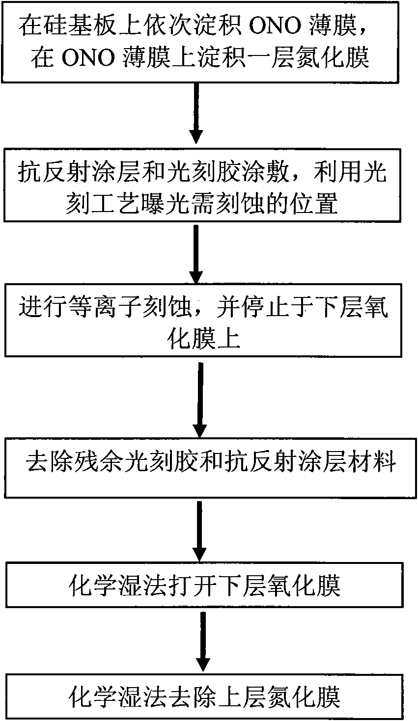
[0022] In order to avoid stripping of the photoresist, the present invention uses a nitride film as a hard mask layer in the last step of etching the oxide film. After all the patterns are defined, the nitride film layer is stripped off to form an ONO structure. Process flow of the present invention such as figure 2 shown.

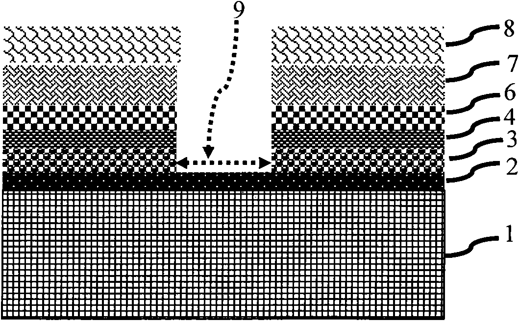
[0023] In the first step, the lower oxide film 2 , the middle oxide nitride film 3 , the upper oxide film 4 and the nitride film 6 are grown sequentially on the silicon substrate 1 . When NONO is grown, the thickness of the nitride film 6 should be less than 200 angstroms, so as to reduce inter-film stress and shorten the final removal time of the nitride film.

[0024] In the second step, the pattern on the photomask is transferred into the photoresist 8 by photolithography. In order to make up for the loss of size 5 caused by the subsequent etching process and chemical wet process, the line size will be compensated during photolithography. After expo...


PUM

PropertyMeasurementUnit
thicknessaaaaaaaaaa

Abstract

The invention discloses a method for producing an ONO structure, comprising the following steps: (1) depositing a lower-layer oxide film, a middle-layer nitric-oxide film and an upper-layer oxide film on a silicon substrate in sequence to form an ONO thin film, and then depositing a nitride film on the formed ONO thin film; (2) coating an anti-reflection coating and photoresist on the nitride film, and then using a photoetching technique to expose a position to be etched; (3) carrying out plasma etching at the position to be etched, and stopping on the lower-layer oxide film; (4) removing the residual photoresist and the anti-reflection coating; (5) further using a wet etching technique to etch the lower-layer oxide film; and (6) removing the residual nitride film by the wet etching technique to form the ONO structure. The structure can solve the problem of peeling off the photoresist, ensure uniformity of etching and effectively control side etching.

Description

technical field [0001] The invention relates to a method for preparing a semiconductor structure, in particular to a method for preparing an ONO (oxide film-oxynitride film-oxide film) structure in a semiconductor SONOS product. Background technique [0002] In SONOS products, ONO structures need to be prepared in specific regions. figure 1 Shown is a schematic diagram of the ONO structure obtained by a common ONO process. In this structure, size 5 represents the reduction in the effective size of the ONO in the ONO process. In order to increase the subsequent process flow and the working window of the device or increase the ONO structure density, the smaller the size 5, the better. [0003] Common ONO structure formation methods in industry include photolithography, plasma etching and chemical wet process. The first step is to use photolithography to define the photoresist pattern, and to compensate for the size change of the ONO line in the subsequent process. In the s...

Claims


Application Information

Patent Timeline
Patent Type & Authority Applications(China)
IPC IPC(8): H01L21/28H01L21/311H01L21/336
Inventor 杨华吕煜坤
Owner SHANGHAI HUA HONG NEC ELECTRONICS
Why Eureka
Try Eureka