Photolithographic technology method of ion implantation layers in HKMG technology

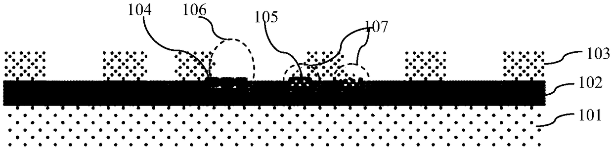
A technology of ion implantation and photolithography, which is applied in the direction of electrical components, semiconductor/solid-state device manufacturing, circuits, etc., can solve the disadvantages; the photoresist will be retained in the area of ​​the dotted circle 106, and the photoresist foot-shaped pattern will be produced , impurity residues, affecting product yield and other problems, to eliminate the defects of photoresist stripping and forming photoresist foot-shaped patterns, and improve the yield

Inactive Publication Date: 2018-08-31
SHANGHAI HUALI INTEGRATED CIRCUTE MFG CO LTD
View PDF5 Cites 0 Cited by
  • Summary
  • Abstract
  • Description
  • Claims
  • Application Information

AI Technical Summary

Problems solved by technology

However, in fact, due to the residual impurities on the surface of the ion implantation layer 102, various adverse effects are often produced on the pattern structure of the photoresist 103.
Photoresist peeling will occur in the region of the dotted circle 106, that is, the photoresist on the top of the acidic chemical substance 104 will be stripped, which is unfavorable for the situation that the photoresist needs to be formed on the top; The photoresist will remain to create a photoresist foot pattern, i.e. the photoresist on top of the alkaline chemistry 105 will remain, which is not good for the situation where the photoresist needs to be removed on top of the alkaline chemistry 105
[0006] It can be seen from the above that the existing method will form photoresist stripping and foot-shaped pattern defects, which will eventually lead to deviations in the definition of ion implantation regions, and finally affect the yield of products

Method used


Image

  • Photolithographic technology method of ion implantation layers in HKMG technology
  • Photolithographic technology method of ion implantation layers in HKMG technology
  • Photolithographic technology method of ion implantation layers in HKMG technology

Examples


Embodiment Construction

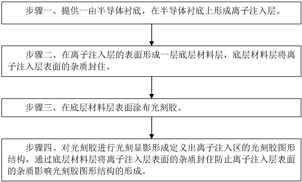
[0028] Such as figure 2 As shown, it is a flow chart of the photolithography process method of the ion implantation layer 2 in the HKMG process of the embodiment of the present invention; as Figure 3A to Figure 3B As shown, it is a structural diagram of each step of the photolithography process method of the ion implantation layer 2 in the HKMG process of the embodiment of the present invention. The photolithography process method of the ion implantation layer 2 in the HKMG process of the embodiment of the present invention includes the following steps:

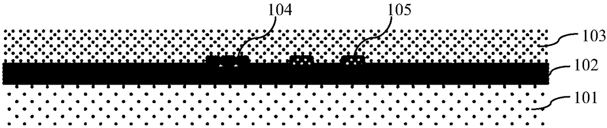
[0029] Step 1, such as Figure 3A As shown, a semiconductor substrate 1 is provided, and an ion implantation layer 2 is formed on the semiconductor substrate 1 .

[0030] In the embodiment of the present invention, the semiconductor substrate 1 is a silicon substrate.

[0031] The ion implantation layer 2 is a material layer for forming the source region and the drain region of the MOSFET with HKMG.

[0032] Step two, su...


PUM


Abstract

The invention discloses a photolithographic technology method of ion implantation layers in HKMG technology. The method comprises steps of step 1, providing a semiconductor substrate and forming an ion implantation layer on the semiconductor substrate; step 2, forming a layer of base layer material layer on the surface of the ion implantation layer, wherein the base layer material layer encapsulates impurities on the surface of the ion implantation layer; step 3, coating photoresist on the surface of the base layer material layer; and step 4, carrying out photolithographic developing on the photoresist so as to form a phoresist graphic structure which defines an ion implantation region, wherein impurities on the surface of the ion implantation layer are encapsulated through the base layermaterial layer so that the impurities on the surface of the ion implantation layer are prevented from influencing the formation of the photoresist graphic structure. According to the invention, impurities on the surface of the ion implantation layer are prevented from influencing the formation of the photoresist graphic structure; particularly, acid chemical substances and alkaline chemical substances can be prevented from influencing the photoresist graphic structure; stripping of the photoresist and defects of photoresist foot-shaped graphics can be separately eliminated; and finally, the yield of the product can be increased.

Description

technical field [0001] The invention relates to a method for manufacturing a semiconductor integrated circuit, in particular to a photolithography process method for an ion implantation layer in an HKMG process. Background technique [0002] HKMG has a gate dielectric layer with a high dielectric constant (HK) and a metal gate (MG), so it is usually abbreviated as HKMG in the art. In the HKMG process, it is necessary to form a high dielectric constant (HK) gate dielectric layer and form a metal gate at the same time. In the existing HKMG process, the metal gate last process is usually used. In the metal gate last process, a dummy polysilicon gate is usually required. That is, the pseudo-polysilicon gate, which uses the pseudo-polysilicon gate to form the gate dielectric layer, channel region, and source-drain region of the device, and then replaces the metal gate, that is, removes the pseudo-polysilicon gate, and fills the removed area of ​​the pseudo-polysilicon gate with m...

Claims


Application Information

Patent Timeline
IPC IPC(8): H01L21/027H01L21/033
CPCH01L21/0274H01L21/0332
Inventor 王耀增黄永发杨尚勇刘隽瀚王志宏许邦泓杨然富
Owner SHANGHAI HUALI INTEGRATED CIRCUTE MFG CO LTD
Why Eureka
Try Eureka