

Encapsulating method of blue-light LED chip
A technology of LED chip and packaging method, which is applied in the direction of electrical components, circuits, semiconductor devices, etc., can solve the problems of many processes, high cost, and low production efficiency, and achieve high process repeatability, short production time, and high packaging efficiency. Effect
- Summary
- Abstract
- Description
- Claims
- Application Information
AI Technical Summary
Problems solved by technology
Method used
Image

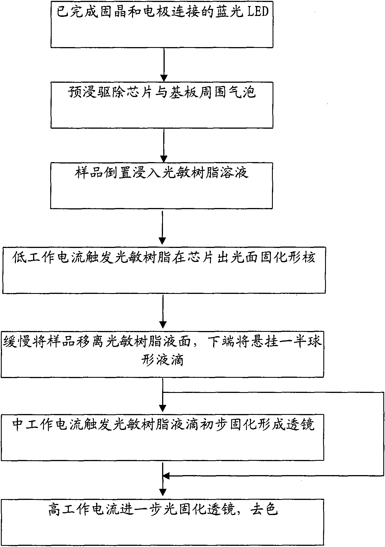
Examples
Embodiment
[0047] Example product test report
[0048] Compare the light color parameters before and after packaging:
[0049] Luminous flux increased from 7.511m before encapsulation to 9.211m after encapsulation;
[0050] Luminous efficacy increased from 6.99lm / w before packaging to 8.821m / w after packaging;
[0051] Optical radiation power increased from 169.09mW before packaging to 208.54mW after packaging;
[0052] The data of color rendering index, dominant wavelength, color purity, peak wavelength, and average wavelength remain unchanged.
[0053] It can be seen that this encapsulation method can effectively improve the indices of luminous flux, luminous efficiency, and radiant power by more than 20%. Moreover, the color rendering, dominant wavelength, color purity, peak wavelength, and average wavelength of the light emitted by the chip can be kept unchanged. This shows that this active packaging method can effectively improve the performance of blue LED chips.
[0054] The ab...
PUM
 Abstract
Description
Claims
Application Information