Photonic crystal all-optical switch

A photonic crystal and all-optical switch technology, applied in optics, nonlinear optics, instruments, etc., can solve problems such as inability to realize photonic crystal all-optical switch, integrated work interference, and no application value, and achieve fast and efficient resonance and mode selection High efficiency of action, energy transfer, making and producing reliable and convenient effects

Inactive Publication Date: 2009-11-04
NANJING UNIV OF POSTS & TELECOMM
View PDF0 Cites 23 Cited by
  • Summary
  • Abstract
  • Description
  • Claims
  • Application Information

AI Technical Summary

Problems solved by technology

[0005] However, the traditional nonlinear photonic crystal optical switch generally only gives a conceptual model based on theoretical derivation. For the defect mode transfer nonlinear photonic crystal optical switch, usually in the photonic crystal containing point defects, the signal light moves along the The XZ cross-section is incident, the control light is vertically incident on the point defect, if the point defect is a nonlinear optical medium, as the control light intensity increases, the refractive index of the medium will change, and the defect in the photonic band gap of the photonic crystal The mode will migrate, and the optical frequency signal that could not pass through may pass now
However, this does not design the photonic crystal all-optical switch from the perspective of the system and consider the transmission characteristics of the optical signal in it. Because controlling the light requires a large light intensity, the impact of the radiated strong light has not been controlled. The integration work will cause direct interference, so the obvious advantages of photonic crystal all-optical switches cannot be realized, and there is no practical application value

Method used


Image

  • Photonic crystal all-optical switch
  • Photonic crystal all-optical switch
  • Photonic crystal all-optical switch

Examples


Embodiment Construction

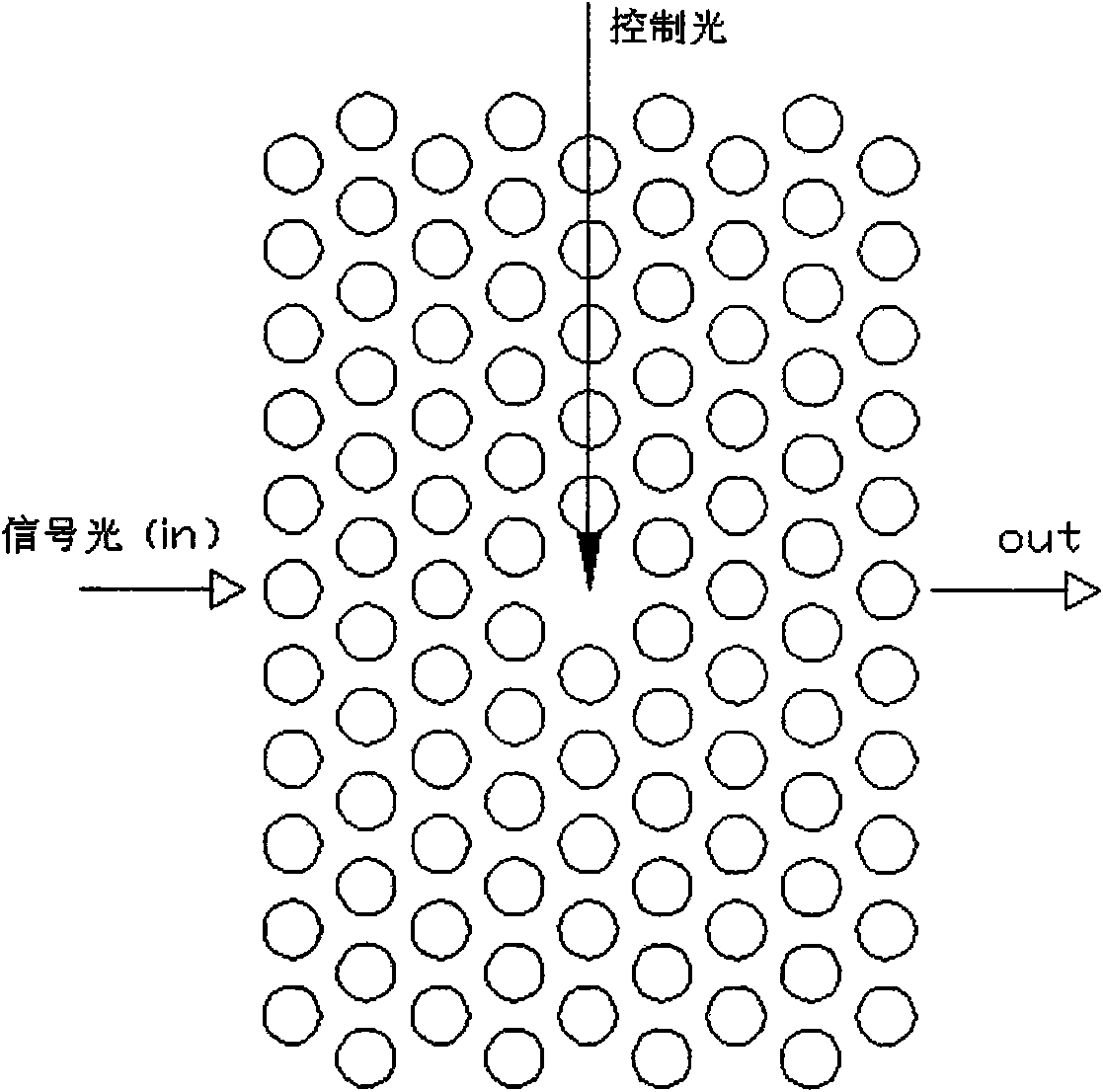
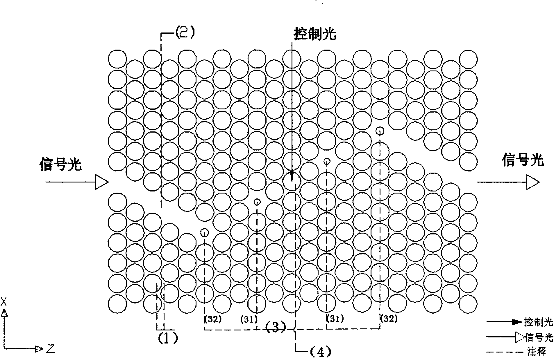
[0018] A photonic crystal all-optical switch provided by the invention is composed of a triangular lattice photonic crystal, a waveguide area, a pulling area, and a nonlinear resonant cavity. Among them, the triangular lattice photonic crystal is a photonic crystal with large air holes distributed periodically in a triangle along the XZ axis. The cross section of the large air holes is circular, and the radius of the large air holes is on the order of the wavelength of light, and the thickness of the plate is the wavelength of light. Order of magnitude, the substrate can be a silicon material; the waveguide region is located at the two ends of the triangular lattice photonic crystal, which is a line defect formed after filling two rows of symmetrical air holes in the triangular lattice photonic crystal (but the two line defects are not connected) ), the filled material is the same as the substrate material, which is a silicon medium, and the end of the waveguide is connected to...


PUM

PropertyMeasurementUnit
refractive indexaaaaaaaaaa

Abstract

A photonic crystal all-optical switch is an all-optical switch (photonic crystal structure), in particular a migrating nonlinear photonic crystal all-optical switch of a defect mode. The photonic crystal all-optical switch comprises triangular lattice photonic crystals (1), a waveguide area (2), a traction area (3) and a nonlinear resonant cavity (4), wherein the triangular lattice photonic crystals (1) are large air hole type photonic crystals in triangular periodic distribution along X and Z axes, symmetric linear defects are introduced at two ends of the triangular lattice photonic crystals to form the waveguide area (2), a central air hole of the triangular lattice photonic crystals (1) is provided with the nonlinear resonant cavity (4), the traction area (3) is arranged between the waveguide area (2) and the nonlinear resonant cavity (4), and signal light is input from the left end of the waveguide area (2) and output from the right end of the waveguide area (2); and control light vertical to the X and Z axes is incident to the central nonlinear resonant cavity (4) along a medium column.

Description

technical field [0001] The invention relates to an all-optical switch (photonic crystal structure), in particular to a defect mode transfer type non-linear photonic crystal all-optical switch, and relates to the technical fields of optical communication and optical information processing. Background technique [0002] With the sharp increase in people's demand for information, communication networks and information computing are facing new challenges, which, to some extent, promote the development of light wave technology. The research on optical information processing technology with optical signal as the calculation object is deepening continuously, among which optical switch can be used as the key device of optical communication switching network and digital optical calculation. At present, a photonic crystal optical switch has become a research feature because of its unique on-off performance. [0003] According to the different light transmission mechanisms, photonic c...

Claims


Application Information

Patent Timeline
Patent Type & Authority Applications(China)
IPC IPC(8): G02F1/365G02F1/361
Inventor 陈鹤鸣王国栋
Owner NANJING UNIV OF POSTS & TELECOMM
Why Eureka
Try Eureka