Emptying signal test circuit for optical storage unit

A technology of signal testing and optical storage, applied in information storage, static storage, recording information storage, etc., can solve the problems of limiting the rapid application of detectors, unable to read optical signals of optical storage sensors well, and tailor-made , to achieve good operability and practicability, easy adjustment of signal parameters, and easy implementation.

Inactive Publication Date: 2012-07-04
EAST CHINA NORMAL UNIV
View PDF2 Cites 0 Cited by
  • Summary
  • Abstract
  • Description
  • Claims
  • Application Information

AI Technical Summary

Problems solved by technology

When the optical storage unit is used as a photon memory, the slow recombination of electron-hole pairs limits the fast read and write of the memory. When the optical storage unit is used as a photodetector, due to the slow recombination process of the above-mentioned electron-hole pairs, the The response of the detector is affected by the previous response, which affects the output of the detector, limiting the rapid application of the detector
[0005] The existing CTIA-type readout circuit is a general-purpose optoelectronic device readout circuit, which itself is not tailor-made according to the basic characteristics of optical storage sensors with low-dimensional quantum dot-quantum well hybrid structures, especially does not provide emptying signal, it cannot read the optical signal of the optical storage sensor with the low-dimensional quantum dot-quantum well hybrid structure well, even if there is a readout circuit for the emptying signal, it cannot easily test the optical storage sensor and the optical storage sensor under different emptying conditions. The working condition of the circuit after docking, because its emptying signal is generated by the reset RS signal, the amplitude is adjusted by the voltage divider, and the width of the signal is fixed

Method used


Image

  • Emptying signal test circuit for optical storage unit
  • Emptying signal test circuit for optical storage unit
  • Emptying signal test circuit for optical storage unit

Examples


Embodiment Construction

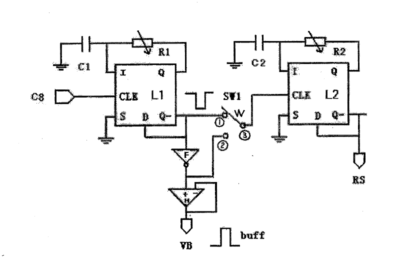
[0019] See attached figure 1 , attached figure 2 And attached image 3 , the present invention is formed by serial connection of two monostable circuits, an inverter F, an operational amplifier H and a gating switch W, the monostable circuit is composed of triggers, capacitors and variable resistors with six ports, and The S terminal of the trigger L1 is grounded; the CLK of the trigger L1 is the output signal of the clock signal terminal connected to the emptying readout circuit; the Q terminal of the trigger L1 is connected in series with the variable resistor R1 and the capacitor C1 and then grounded; the I of the trigger L1 The terminals are connected to the variable resistor R1 and the capacitor C1 in common; the Q-terminal of the trigger L1 respectively contacts the D terminal of the trigger L1, the input terminal of the inverter F and the ① terminal of the strobe switch W; the output terminal of the inverter F Connect the positive pole of the operational amplifier H ...


PUM


Abstract

The invention discloses an emptying signal test circuit for an optical storage unit, which is characterized in that the emptying signal test circuit is formed by serially connecting two monostable circuits, an inverter F, an operational amplifier H and a gating switch, wherein the monostable circuit consists of a double-D trigger with six ports, a capacitor and a variable resistor; and an output signal from an emptying reading circuit is accessed to the first monostable circuit, is used as a VB signal output and a signal input of the next monostable circuit after being processed by the inverter and the operational amplifier, and finally is output as an RS signal. An emptying signal of the test circuit is generated independently by another circuit and is not dependent on a reset signal; andthe test circuit can flexibly adjust the time of emptying pulse, the width of signals and the positions of the emptying signal and the reset signal for the convenience of testing the working conditions after an optical storage sensor is butted with the circuit under different emptying conditions; and compared with the prior art, the test circuit has the advantages of good operability and practicability, and convenient adjustment of signal parameters.

Description

technical field [0001] The invention relates to the technical field of electronics and circuit design, in particular to an empty signal test circuit for an optical storage unit. Background technique [0002] Optical storage technology reads and writes data through optical methods, and the photodetector detects changes in light intensity and polarization direction to read out the data in the storage unit. The main function of the readout circuit (ROIC) is to preprocess the weak signals of the storage, detection or imaging unit in the optoelectronic device (such as integration, amplification, filtering, sampling / holding, etc.) and provide an interface between signal processing stages. [0003] When the specially designed semiconductor low-dimensional structure is excited by light, the incident photons can be converted into space-separated electron-hole pairs and stored for a long time. In the semiconductor optical storage unit with quantum well-quantum dot composite structure...

Claims


Application Information

Patent Timeline
Patent Type & Authority Patents(China)
IPC IPC(8): G11C29/00H03K3/033H03K3/017H03K5/00G11B7/00
Inventor 韩建强郭方敏詹国钟熊大元越方禹朱自强褚君浩
Owner EAST CHINA NORMAL UNIV
Why Eureka
Try Eureka