Supercharge Your Innovation With Domain-Expert AI Agents!

Plasma display device

A technology of plasma display panel and display device, applied in static indicators, instruments, etc., can solve the problem of increasing the length of the addressing period and the like

Inactive Publication Date: 2009-11-18
LG ELECTRONICS INC
View PDF0 Cites 2 Cited by
  • Summary
  • Abstract
  • Description
  • Claims
  • Application Information

AI Technical Summary

Problems solved by technology

[0003] As the size and resolution of the PDP increase, the length of the addressing period increases

Method used


Image

  • Plasma display device
  • Plasma display device
  • Plasma display device

Examples


Embodiment Construction

[0036] The present invention will be described more fully hereinafter with reference to the accompanying drawings, in which exemplary embodiments of the invention are shown.

[0037] Hereinafter, the present invention will be described in detail with reference to the accompanying drawings, in which exemplary embodiments of the invention are shown.

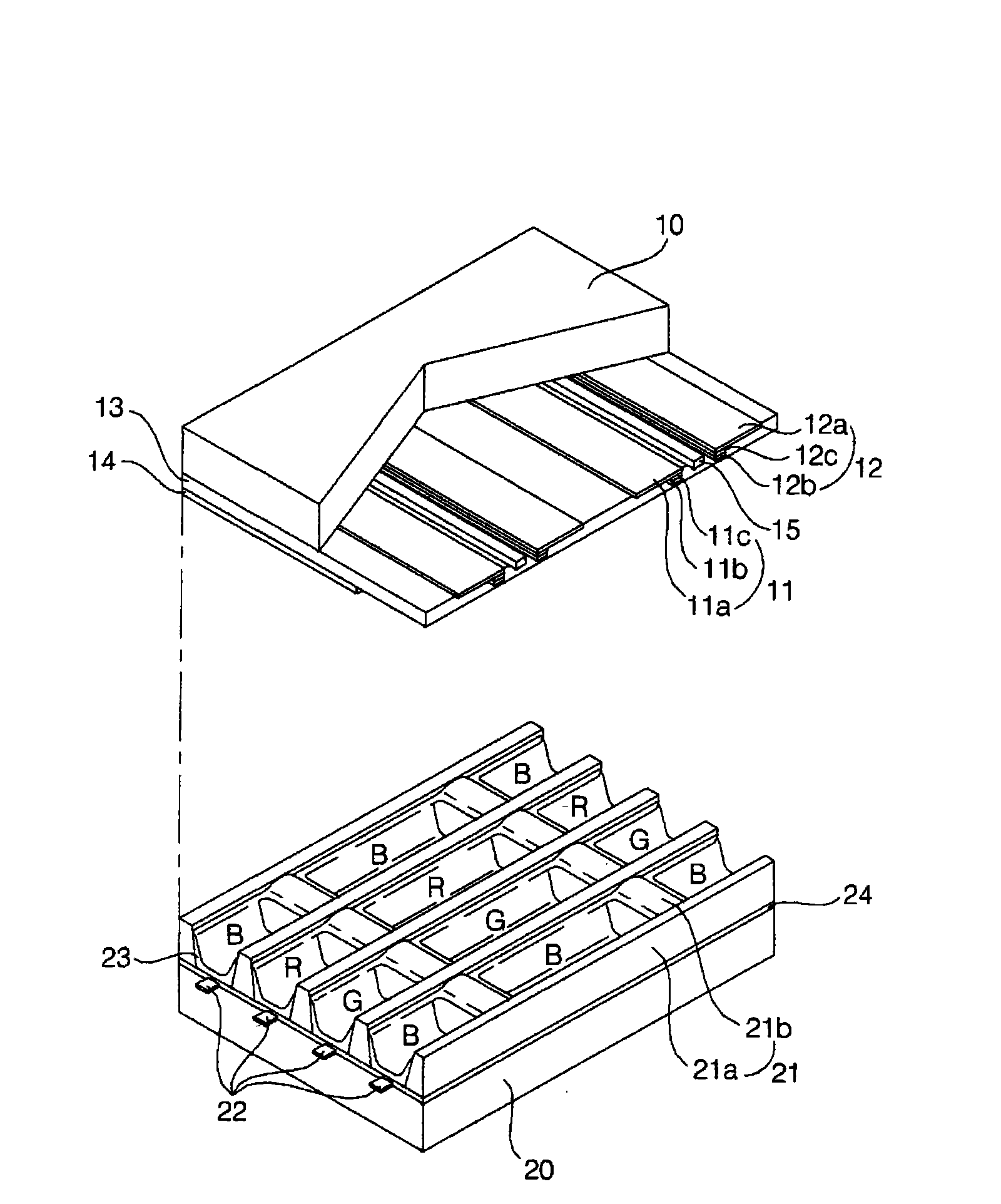
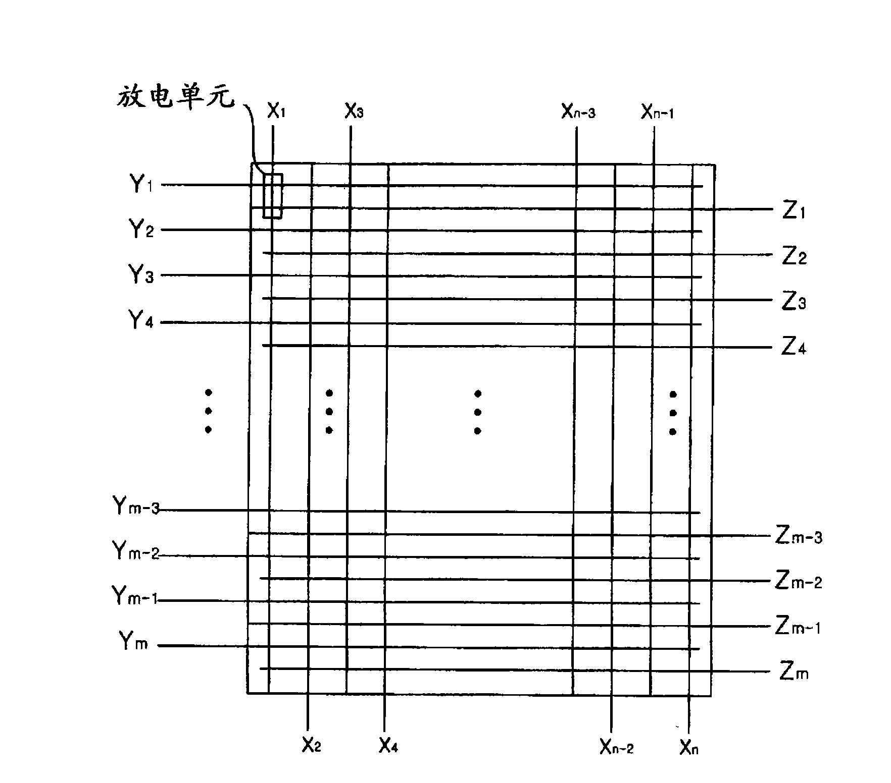
[0038] figure 1 A perspective view illustrating a display device according to an embodiment of the present invention is illustrated. refer to figure 1 , a plasma display panel (PDP) includes: an upper substrate 10; a plurality of electrode pairs formed on the upper substrate 10, respectively composed of scan electrodes 11 and sustain electrodes 12; a lower substrate 20; and a plurality of electrode pairs formed on the lower substrate 20 Address electrodes 22 .

[0039] Each of the electrode pairs includes transparent electrodes 11a and 12a and bus electrodes 11b and 12b. The transparent electrodes 11a and 12a may be formed of i...


PUM


Abstract

A plasma display device is provided. In the plasma display device, a plurality of scan electrodes are divided into one or more scan electrode groups, and different driving signals are applied to the scan electrode groups. More specifically, different scan bias voltages are applied to the scan electrodes during a scan period, and different signals are applied to the scan electrodes during a set-down period of a reset period. Therefore, it is possible to stabilize an address discharge in scan electrodes to which scan signals are applied late.

Description

technical field [0001] The present invention relates to a plasma display device, and more particularly, to a driving signal for driving a plasma display panel included in the plasma display device. Background technique [0002] Generally, a plasma display panel (PDP) includes an upper substrate, a lower substrate, and a plurality of partition walls arranged between the upper substrate and the lower substrate and defining a plurality of cells, each of which is filled with a material such as neon (Ne) , the main discharge gas of helium (He) or a mixed gas of neon and helium (Ne+He), and an inert gas containing a small amount of xenon. When a discharge occurs due to a high-frequency voltage, the inert gas generates vacuum ultraviolet (UV) rays, and the UV rays excite phosphor layers between partition walls, thereby realizing an image. The PDP is thin and lightweight, and has long been expected to become a dominant next-generation display device. [0003] As the size and resol...

Claims


Application Information

Patent Timeline
IPC IPC(8): G09G3/28G09G3/288G09G3/293
CPCG09G2310/0267G09G3/293G09G2310/066G09G2310/0218G09G3/296
Inventor 崔允畅姜成昊李东洙玉治软
Owner LG ELECTRONICS INC
Features
  • R&D
  • Intellectual Property
  • Life Sciences
  • Materials
  • Tech Scout
  • Unparalleled Data Quality
  • Higher Quality Content
  • 60% Fewer Hallucinations
Learn More