

Vertical GaN-based LED chip and manufacture method thereof
A technology of LED chip and manufacturing method, which is applied in the direction of electrical components, circuits, semiconductor devices, etc., can solve the problems of low good rate and consistency, chip damage, etc., and achieve high utilization rate, accelerated processing speed, and good chip current expansion Effect
- Summary
- Abstract
- Description
- Claims
- Application Information
AI Technical Summary
Problems solved by technology
Method used
Image

Examples
Embodiment Construction
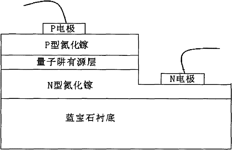
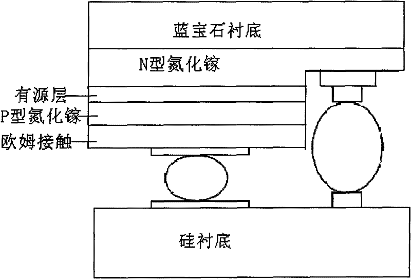
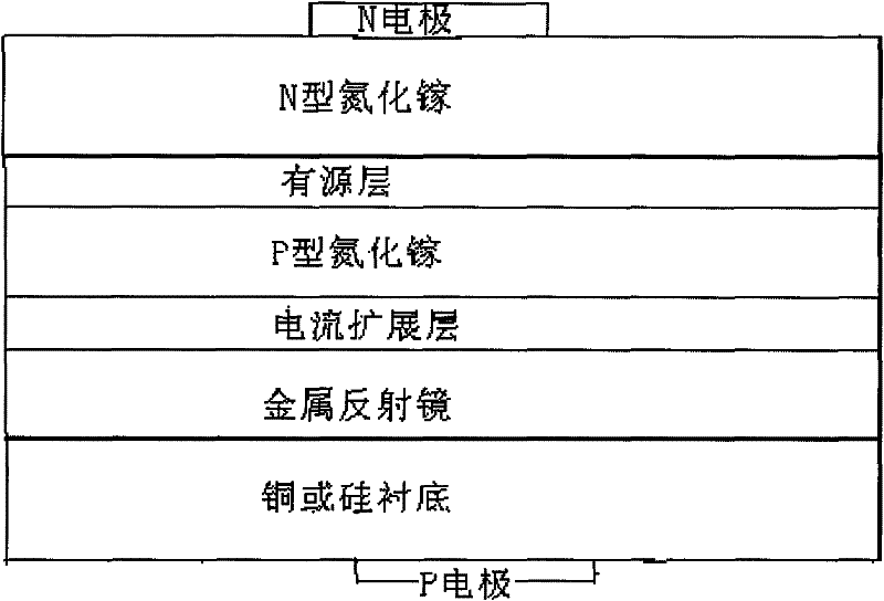
[0031] Such as Figure 4As shown, the vertical GaN-based LED chip of the present invention includes sapphire or 6H-SiC transparent substrate, N-type GaN, quantum well active layer, P-type GaN, current spreading layer, metal reflector, bonding Welding layer and conductive substrate, on which a P electrode is made, and a window up to the N-type GaN layer is provided on the sapphire or 6H-SiC transparent substrate, and a layer of metal is vapor-deposited in the window, and on this metal layer An N electrode is drawn out.
[0032] In order to further improve the light extraction efficiency of the chip, it can be as Figure 5 The light-emitting surface of the sapphire or 6H-SiC transparent substrate of the fabricated vertical GaN-based LED chip is processed into a rough surface to reduce the internal total reflection of light and destroy the total reflection. or as Image 6 As shown, for the sapphire substrate of the vertical GaN-based LED chip, the photonic crystal is produced ...
PUM
 Abstract
Description
Claims
Application Information