Solid-state imaging device, driving method thereof, and camera

A solid-state imaging device and pixel technology, applied in solid-state image signal generators, image communications, televisions, etc., can solve problems such as hindering high-speed frame rate, increased power consumption, and increased chip area, achieving high practical value , Low power consumption, high S/N ratio effect

Inactive Publication Date: 2009-12-23
PANASONIC CORP
View PDF11 Cites 29 Cited by
  • Summary
  • Abstract
  • Description
  • Claims
  • Application Information

AI Technical Summary

Problems solved by technology

[0007] However, a problem in the conventional method of increasing the number of bits of the AD converter for white balance is that, for example, as described in the above-mentioned Patent Document 2, a ramp waveform is used for the reference signal, and the reference signal changes until the corresponding When the comparator in the column shows that the pixel signal matches the reference signal, the counting clock increases, and the time it takes to count in the AD conversion method increases.
For example, to increase 1 bit, the AD conversion time will be doubled, which hinders the high-speed frame rate.
Also, for multi-bit, it is conceivable to use a plurality of the above-mentioned comparator circuits and perform parallel processing. In this case, the problem that occurs due to the increase of the circuit scale is that the chip area increases or the power consumption increases. Big and so on
In addition, in order to increase the number of bits of the AD converter, it is also considered that the frequency of the clock that can be used for conversion is increased, so there is a problem that the clock speed reaches the limit or the power consumption due to high-speed driving increases.
[0008] In addition, in the technique of the above-mentioned Patent Document 1, complex control such as appropriately changing the resistance values ​​of the variable resistors VR1 to VR4 or switching the switches SW1 to SW4 in accordance with the colors assigned to the readout pixels is required.
[0009] In addition, the problem in the technique of the above-mentioned Patent Document 2 is that the gain is adjusted for each color by changing the inclination of the ramp waveform. When a large gain is required, the inclination of the ramp waveform needs to be very small. In this way, the 1-bit comparison voltage used to compare the pixel signal and the reference signal will be reduced, that is to say, the weighted voltage will be reduced, resulting in an increase in the error during AD conversion and a decrease in the S / N ratio (signal / noise ratio). Difference

Method used


Image

  • Solid-state imaging device, driving method thereof, and camera
  • Solid-state imaging device, driving method thereof, and camera
  • Solid-state imaging device, driving method thereof, and camera

Examples


Embodiment 1

[0053] First, Embodiment 1 of the present invention will be described.

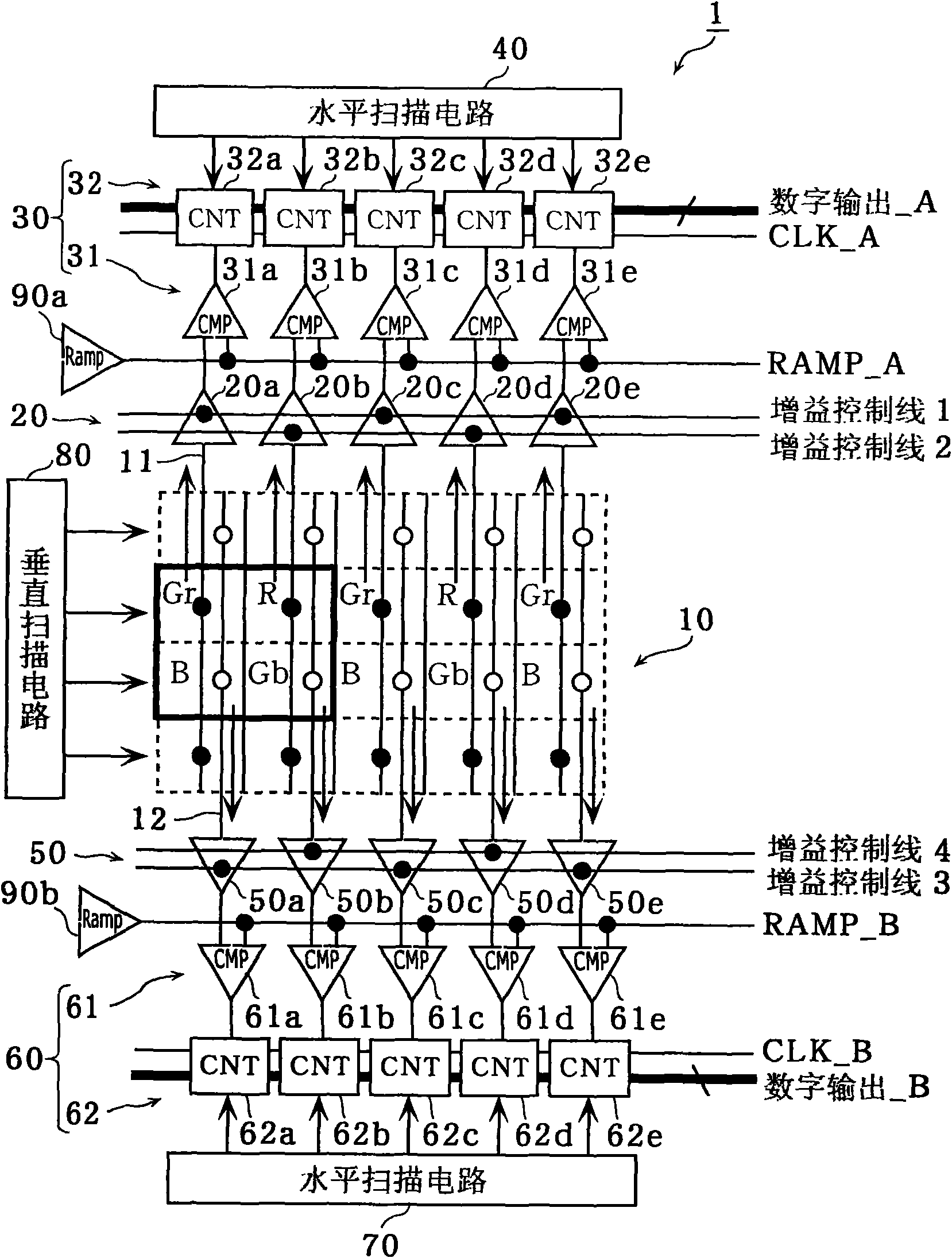
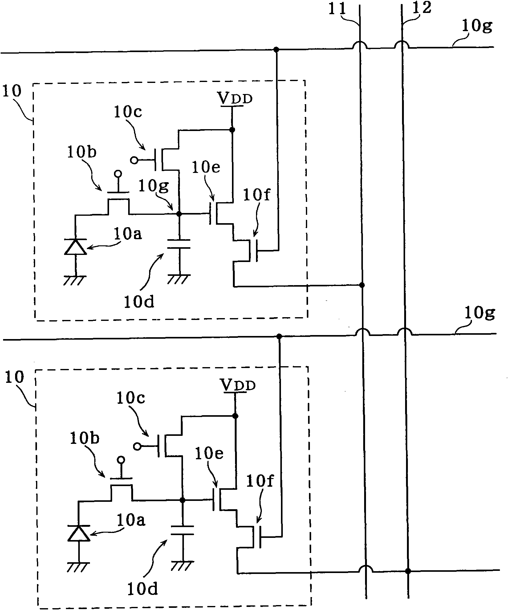
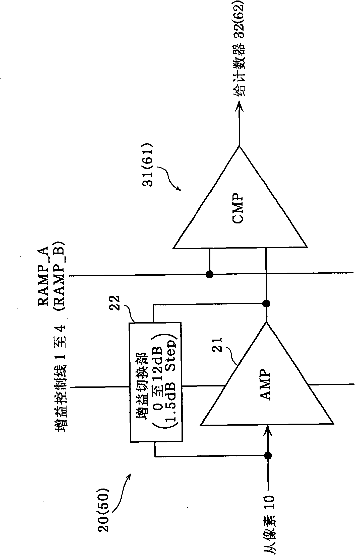
[0054] figure 1 It is a circuit block diagram of the solid-state imaging device 1 in Embodiment 1 of the present invention. This solid-state imaging device 1 is a color image sensor having a plurality of pixels 10 that convert light into electrical signals formed on one semiconductor substrate, and is characterized by, for example, RGB (red, blue, green) A plurality of column amplifiers 20 (20a to 20e) and 50 (50a to 50e) independent for each color, and a plurality of column AD converters 30 (31a to 31e, 32a to 32e) and 60 independent for each color (61a to 61e, 62a to 62e), the plurality of column AD converters 30 and 60 have comparator sections 31 (31a to 31e) and 61 (61a to 61e) for comparing signals and pass through the comparator 31 and 61 compare the pixel signal and the ramp wave to count the counter parts 32 (32a to 32e) and 62 (62a to 62e) of the clock until a predetermined time, and the solid...

Embodiment 2

[0093] Hereinafter, Example 2 of the present invention will be described.

[0094] Figure 10 It is a circuit block diagram of the solid-state imaging device 2 in Embodiment 2 of the present invention. The solid-state imaging device 2 is characterized in that different column AD converter gains can be set according to each color of RGB, and the solid-state imaging device 2 includes: a plurality of pixels 10, a plurality of column amplifiers 20 and 50, and a plurality of column AD converters. Converters 30 and 60 , horizontal scanning circuits 40 and 70 , vertical scanning circuit 80 , and ramp wave generating sections 91 to 94 .

[0095] This solid-state imaging device 2 is different from Embodiment 1 in that it has four ramp wave generating sections 91 to 94 instead of the two ramp wave generating sections 90a and 90b in Embodiment 1, and the rest is the same as that of Embodiment 1. same. Hereinafter, the same reference numerals are assigned to the same configurations as ...


PUM


Abstract

A solid-state imaging device which optimizes gains for each color without a need for complicated control of changing the resistance values of variable resistances and switching switches depending on pixels from which signals are to be read, while preventing an S / N deterioration in AD conversion. The solid-state imaging device comprises: a plurality of pixels arranged in a matrix; column amplifiers, each amplifying signals generated by pixels of a corresponding one of columns of the matrix; and column AD converters, each performing AD conversion on a signal generated by a corresponding one of the column amplifiers, wherein each of the plurality of pixels corresponds to a color among colors, and each of the column amplifiers amplifies output signals generated by all pixels of a corresponding one of the colors, among pixels of the corresponding column of the matrix.

Description

technical field [0001] The present invention relates to a solid-state imaging device that converts light into electrical signals, and more particularly to a solid-state imaging device that includes an amplifier and an analog-to-digital converter for each column of a plurality of pixels arranged in a matrix. Background technique [0002] In a solid-state imaging device (color image sensor) capable of supporting colors, it is necessary to adjust the white balance in accordance with changes in the color temperature of an object or the like. For example, the color of the subject changes depending on the type of light (sunlight, fluorescent lamp, etc.), so it is necessary to process it in the solid-state imaging device so that the white color of the subject corresponds to the color temperature at this time. It is also white in the image signal. [0003] In the past, in order to adjust the white balance, either increase the number of bits (resolution) of the A / D converter and use...

Claims


Application Information

Patent Timeline
Patent Type & Authority Applications(China)
IPC IPC(8): H04N9/083H04N3/15H04N5/225H04N9/04
CPCH04N9/045H04N9/735H04N5/378H04N25/70H04N25/75H04N25/134H04N23/88
Inventor 桝山雅之京极正法
Owner PANASONIC CORP
Why Eureka
Try Eureka