Light-emitting diode chip and preparation method thereof

A technology of light-emitting diodes and chips, which is applied in the manufacturing of semiconductor/solid-state devices, electrical components, and electrical solid-state devices, etc., can solve the problems of non-separation of thermoelectricity, unfavorable chip heat dissipation, etc., to reduce light loss, improve heat dissipation effect, reduce absorption or reflection effect

Inactive Publication Date: 2009-12-30
HE SHAN LIDE ELECTRONICS ENTERPRISE CO LTD
View PDF1 Cites 19 Cited by
  • Summary
  • Abstract
  • Description
  • Claims
  • Application Information

AI Technical Summary

Problems solved by technology

For this reason, the applicant has applied for a patent on a light-emitting diode and its preparation method. The light-emitting diode in this patent has adopted a single-electrode chip with a vertical structure and removed the substrate of the bare core on the chip. It improves the luminous efficiency and eliminates the influence of the substrate on the chip, but because the heat sink substrate is made of conductive materials, and the two electrode layers connected to the external power line are respectively arranged on the back of the heat sink substrate and the n-type On the semiconductor layer, the heat sink substrate acts as a heat sink substrate and conducts electricity as an electrode at the same time, that is, "thermoelectricity is not separated". This structure is not conducive to the heat dissipation of the chip because the substrate conducts heat and conducts current at the same time.
There is also a light-emitting diode chip structure disclosed in Japanese Patent JP2003-142736. Although it arranges two separated auxiliary electrodes connected to the bare core on the heat sink substrate, its substrate 12 acts as a heat dissipation substrate while It should also be used as an electrode to conduct electricity, so there are also problems such as thermoelectricity not being separated, which is not conducive to chip heat dissipation.

Method used


Image

  • Light-emitting diode chip and preparation method thereof
  • Light-emitting diode chip and preparation method thereof
  • Light-emitting diode chip and preparation method thereof

Examples


Embodiment I

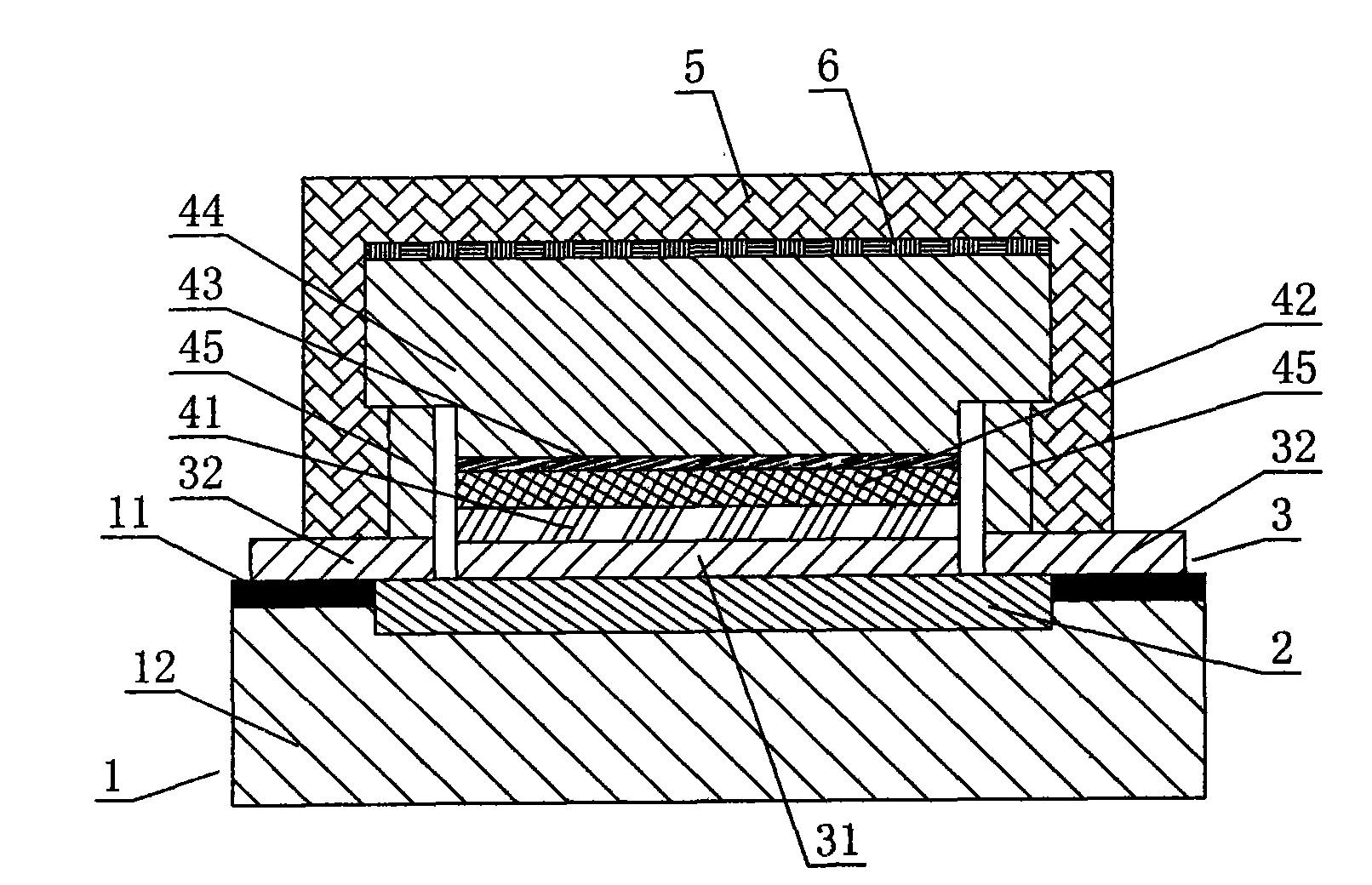
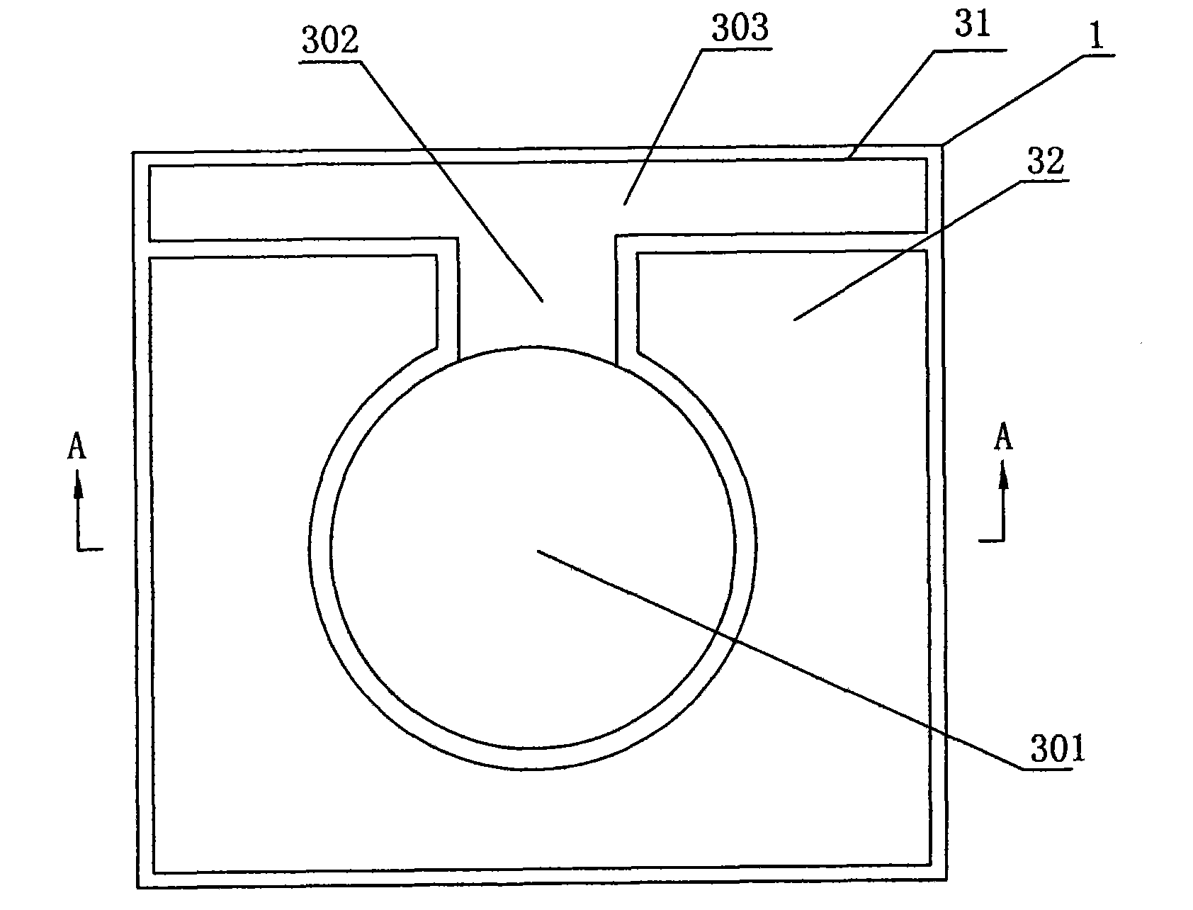
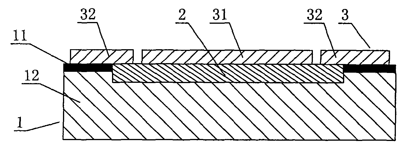
[0061] Embodiment I: first refer to figure 1 and Figure 1A-Figure 1G A method of manufacturing a light emitting diode chip according to an embodiment of the present invention is described. Such as Figure 1A , Figure 1B As shown, a heat sink substrate 1 with an insulating layer on the upper surface is first prepared, and then a metal bonding layer 3 is formed on the upper surface of the heat sink substrate 1 by methods such as sputtering and electroplating, and the metal bonding layer 3 is patterned as A first bonding layer 31 and a second bonding layer 32 isolated from each other are formed, wherein the first bonding layer 31 includes a circular central portion 301 and a ring extending outward from one side of the circular central portion 301 for connecting with a circumscribed The lead-out part 302 and the welding wire part 303 connected by the power line, the second bonding layer 32 surrounds the surrounding position of the first bonding layer 31 in an incomplete manne...

Embodiment II

[0066] Embodiment II: as figure 2 and 2A - Figure 2F shown, refer to Figure 2A , Figure 2B , first prepare the heat sink substrate 1 with the insulating layer 11 on the upper surface. A metal bonding layer is formed on the upper surface of the heat sink substrate 1 by methods such as sputtering and electroplating, and the metal bonding layer is patterned into a first bonding layer 31 formed on the left part and a second bonding layer on the right part. 32, the first bonding layer 31 and the second bonding layer 32 are isolated from each other. The material of the metal bonding layer 3 is selected from Al, Ag, Pt, Cr, Mo, W, Au, Cu, Ni, BeAu or combinations thereof. Optionally, an electrostatic discharge ESD layer 2 of double Zener diodes can also be formed on the upper surface of the heat sink substrate 1, such as Figure 1B shown. The preferred manufacturing method of the above-mentioned heat sink substrate 1 is: first make the bottom plate 12 of the heat sink subs...

Embodiment III

[0072] Embodiment III: as image 3 and Figure 3A-3D As shown, the present invention also provides a method for manufacturing a high-power light-emitting diode chip. refer to Figure 3A Firstly, a heat sink substrate 1 with an insulating layer on the upper surface is prepared. Then, on the upper surface of the heat sink substrate 1, a metal bonding layer 3 is formed by methods such as sputtering and electroplating, and the metal bonding layer 3 is patterned into a first bonding layer 31 and a second bonding layer 31 that are separated from each other and interspersed with each other. The bonding layer 32, wherein the first bonding region 31 includes a plurality of small bonding regions 311 and a lead-out portion 314 that connects the ends of each small bonding layer 311 and extends to the side of the bare core 4 for connecting to an external power supply line and The welding wire part 313, and a plurality of circular metal contact bosses 312 distributed in a matrix are arra...


PUM


Abstract

The invention relates to a light-emitting diode chip, which comprises a heat sink substrate, a metal joint layer and a bare core, wherein the bare core comprises an n-type semiconductor layer, a luminous layer, a p-type semiconductor layer, a reflecting layer and an electrode layer; and the light-emitting diode chip is characterized in that: the metal joint layer comprises a first joint layer and a second joint layer which are mutually separated and can be connected with an external power line; the first joint layer is jointed with the reflecting layer; the second joint layer is jointed with the electrode layer; at least the contact part of the upper surface of the heat sink substrate and the metal joint layer is set as an insulation part; and the bare core is connected with the external power line through the first joint layer and the second joint layer to form a current passage with thermal-electric separation. The light-emitting diode chip adopts a thermal-electric separating structure, so that the heat sink substrate is specially used for radiating, and a conduction part is completed by a metal joint layer composition, so the radiating effect is obviously improved, and simultaneously the luminous efficiency is correspondingly improved. The invention also relates to a preparation method for the light-emitting diode chip.

Description

technical field [0001] The invention relates to a light emitting diode (LED) chip and a preparation method thereof. Background technique [0002] The traditional light-emitting diode chip is placed on a bottom plate (substrate) with the electrode metal facing upward, so the light-emitting layer of the light-emitting diode chip is below the electrode metal layer, and part of the emitted light is absorbed by the electrode metal layer, thereby affecting the light emission. The light extraction efficiency of the diode. With the continuous development of semiconductor chip (chip) technology, the traditional technology can no longer meet the increasing requirements for the luminous efficiency and brightness of light emitting diodes. In order to improve the light extraction efficiency of light emitting diodes, flip chip (flip chip) technology is widely used in the preparation of light emitting diodes. Since the light-emitting diodes prepared by the flip-chip process have the char...

Claims


Application Information

Patent Timeline
Patent Type & Authority Applications(China)
IPC IPC(8): H01L25/075H01L33/00H01L21/48H01L21/50H01L33/10H01L33/36
Inventor 樊邦扬翁新川
Owner HE SHAN LIDE ELECTRONICS ENTERPRISE CO LTD
Why Eureka
Try Eureka