Optical membrane structure and manufacturing method thereof

A technology of optical film and manufacturing method, which is applied in optics, optical components, nonlinear optics, etc., and can solve the problems of affecting test results, appearance defects, and low yield

Inactive Publication Date: 2010-02-10
ENTIRE TECH CO LTD
View PDF0 Cites 19 Cited by
  • Summary
  • Abstract
  • Description
  • Claims
  • Application Information

AI Technical Summary

Problems solved by technology

Furthermore, the manufacturing method of the rhombic lens uses optical glue to transfer the shape on the mold to the base material. It must go through operations such as gluing, pressing, hardening and forming, and release. However, in the process of release, it is easy to Due to improper operation, appearance defects are caused, so the manufacturing method is not only complicated, but also the production process is difficult, resulting in low yield
[0005] In addition, due to the difference in shrinkage between the base material and the forming rubber, the rhombus sheet will warp during the reliability test, which will affect the test results
In the structure of the existing rhombic sheet, it is necessary to use ultraviolet curing paint to form on the base material, which often causes scratches, poor release and defects, and the process is complicated and the production yield is low.

Method used


Image

  • Optical membrane structure and manufacturing method thereof
  • Optical membrane structure and manufacturing method thereof
  • Optical membrane structure and manufacturing method thereof

Examples


Embodiment Construction

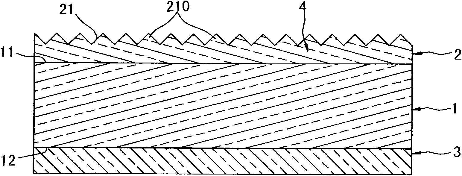
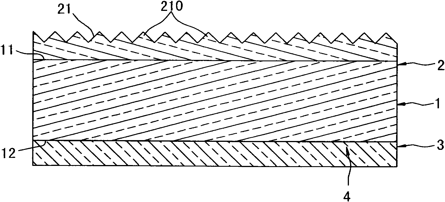
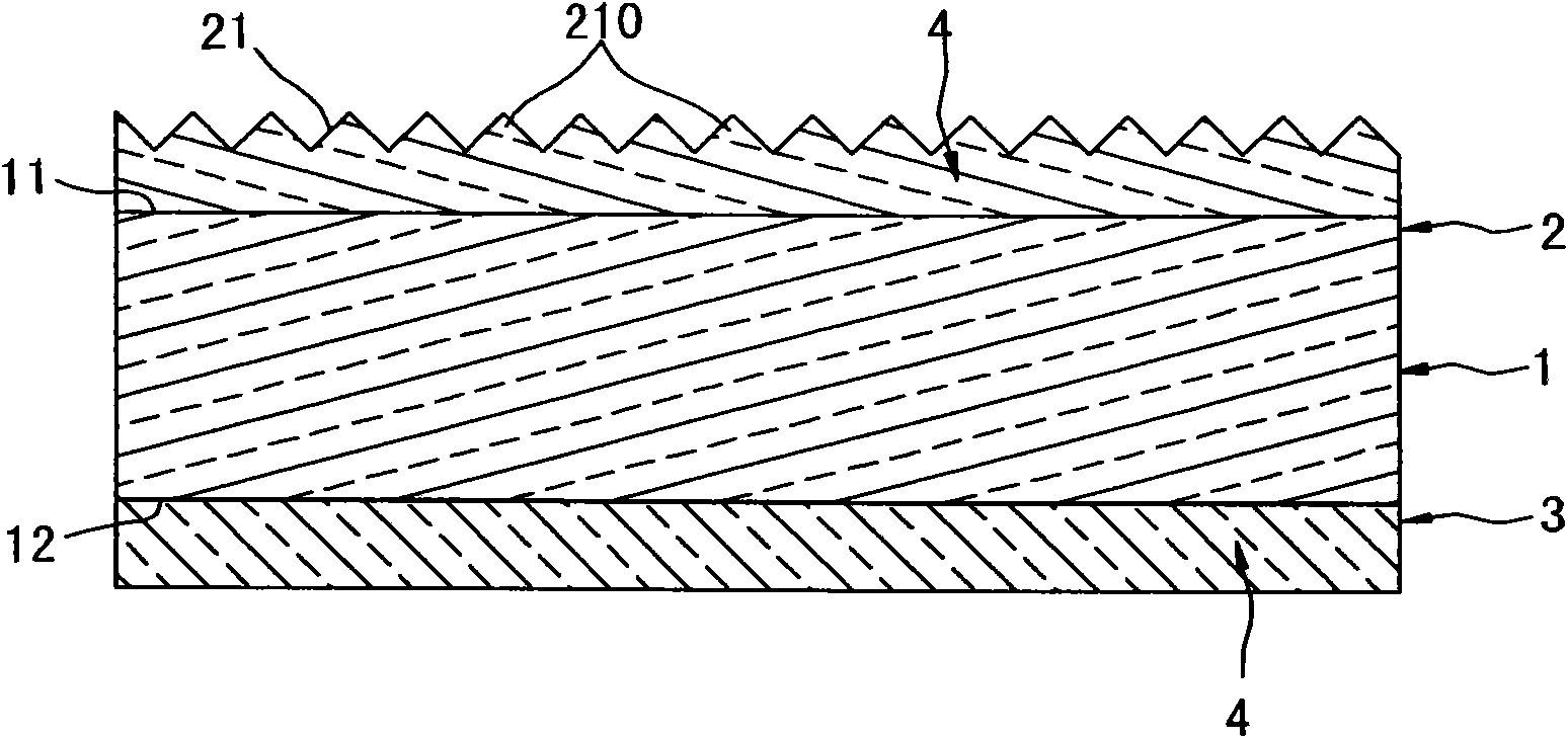
[0033] see figure 1 As shown, it is a schematic view of the first embodiment of the structure of the optical film of the present invention, and its structure includes: a base material layer 1 , a first light-transmitting layer 2 and a second light-transmitting layer 3 . Through the co-extrusion process, the substrate layer 1 , the first and second transparent layers 2 and 3 can be combined into one. Wherein, the substrate layer 1, the first and the second light-transmitting layers 2, 3 are plastic materials, and the plastic materials can be polystyrene (PS), polymethyl methacrylate-polystyrene copolymer (MS) , polycarbonate (PC), polyethylene terephthalate (PET), COP, polypropylene (PP) or acrylic (PMMA) or plastic materials equivalent to the above materials.

[0034] The substrate layer 1 is the main structure of the optical film structure, which has a light-emitting surface 11 and a light-incident surface 12 opposite to the light-emitting surface 11, serving as the bonding ...


PUM

PropertyMeasurementUnit
diameteraaaaaaaaaa

Abstract

The invention provides an optical membrane structure and a manufacturing method thereof. The manufacturing method is characterized in that: through a coextrusion process, a main substrate, a first transmission material and a second transmission material are combined into a whole to change the light advancing direction; in a rolling mode, a light guide microstructure is formed on the surface of thefirst transmission material directly; moreover, at least one layer or each layer of the main substrate, the first transmission material and the second transmission material is added with dispersion particles to form the optical membrane structure with scratch resistance and high production yield. Therefore, the invention can provide the optical membrane structure with high evenness; the structurecan be effectively prevented from structural warpage generated due to environmental change through coextrusion integral formation; and the improved optical membrane with scratch resistance and high production yield is formed through the design of the surface dispersion particles.

Description

technical field [0001] The present invention relates to an optical film structure and a manufacturing method thereof, in particular to an optical film structure with different structures and shapes and a manufacturing method thereof through the arrangement of different three-dimensional structures and diffusing particles, so as to change the path of light, And by adding diffusion particles on the surface of the three-dimensional structure, the diffusion effect can be used to avoid production defects of the optical film structure and effectively improve the production yield. Background technique [0002] With the development of digital TV, in recent years, in the competition in the field of display, liquid crystal display continues to be valued by consumers and industry players, and the sales volume of the product also maintains a high growth rate. Among them, the imaging method of the liquid crystal display is driven by the switch of the electric field and displays a high-qu...

Claims


Application Information

Patent Timeline
Patent Type & Authority Applications(China)
IPC IPC(8): G02B5/02G02B1/04G02F1/13357
Inventor 张裕伟李开新谢承祐
Owner ENTIRE TECH CO LTD
Why Eureka
Try Eureka