Soft support bridge type silicon micro-piezoelectric microphone chip and prepration method thereof
An electric microphone and soft support bridge technology, applied in piezoelectric/electrostrictive transducer microphones, piezoelectric/electrostrictive/magnetostrictive devices, sensors, etc., can solve the problems of low sensitivity and low sensitivity of microphones
- Summary
- Abstract
- Description
- Claims
- Application Information
AI Technical Summary
Problems solved by technology
Method used
Image
Examples
Embodiment 1
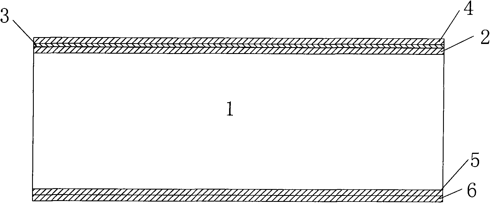
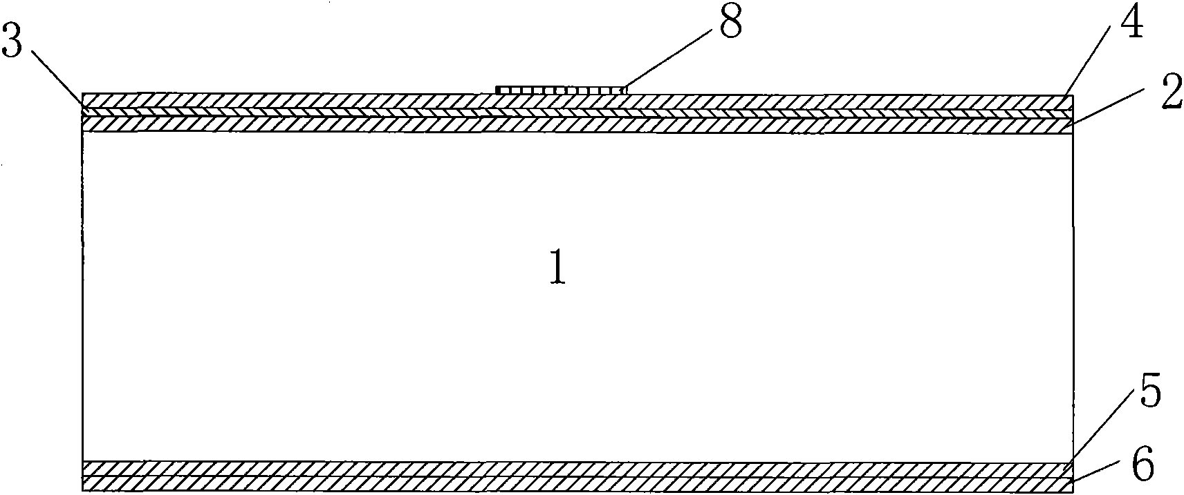
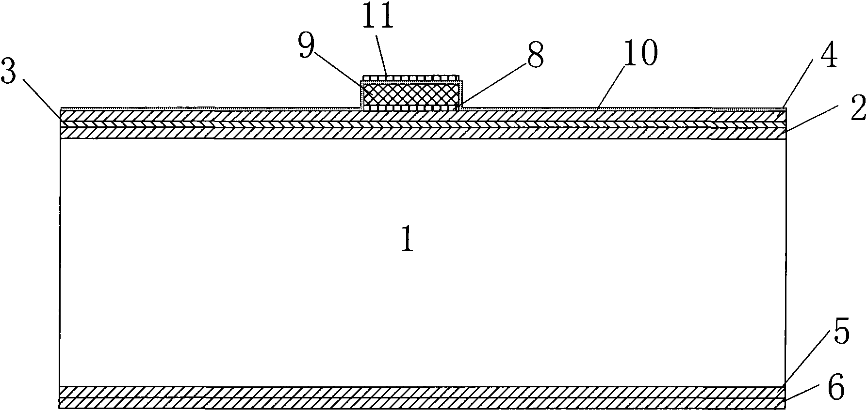
[0061] Embodiment 1, adopt preparation method of the present invention to prepare a soft support bridge type silicon micro piezoelectric microphone chip, its steps are as follows:
[0062] 1) Clean the silicon substrate 1
[0063] Cleaning the silicon substrate 1 with an acid cleaning solution and an alkaline cleaning solution respectively, and then rinsing it with deionized water;
[0064] 2) depositing the first silicon nitride film layer 2
[0065] Depositing a first silicon nitride film layer 2 with a thickness of 0.5 μm on the front side of the silicon substrate 1 and a silicon nitride mask layer 5 with a thickness of 0.5 μm on the back surface of the silicon substrate 1 by using low-pressure chemical vapor deposition equipment;
[0066] 3) Deposit silicon dioxide film layer 3
[0067] Depositing a silicon dioxide film layer 3 with a thickness of 0.2 μm on the first silicon nitride film layer 2 by using plasma-assisted chemical vapor deposition equipment;
[0068] 4) D...
Embodiment 2
[0087] Embodiment 2, adopting the preparation method of the present invention to prepare a soft support bridge type silicon micro piezoelectric microphone chip, its steps are as follows:
[0088] 1) Clean the silicon substrate 1
[0089] Cleaning the silicon substrate 1 with an acid cleaning solution and an alkaline cleaning solution respectively, and then rinsing it with deionized water;
[0090] 2) depositing the first silicon nitride film layer 2
[0091] Deposit the first silicon nitride film layer 2 with a thickness of 0.5 μm on the front side of the silicon substrate 1 and the third silicon nitride mask layer 5 with a thickness of 0.5 μm on the back surface of the silicon substrate 1 by using low-pressure chemical vapor deposition equipment ;
[0092] 3) Deposit silicon dioxide film layer 3
[0093] Depositing a silicon dioxide film layer 3 with a thickness of 0.5 μm on the first silicon nitride film layer 2 by using plasma-assisted chemical vapor deposition equipment...
Embodiment 3
[0113] Embodiment 3, adopting the preparation method of the present invention to prepare a soft support bridge type silicon micro piezoelectric microphone chip, its steps are as follows:
[0114] 1) Clean the silicon substrate 1
[0115] Cleaning the silicon substrate 1 with an acid cleaning solution and an alkaline cleaning solution respectively, and then rinsing it with deionized water;
[0116] 2) depositing the first silicon nitride film layer 2
[0117] Deposit the first silicon nitride film layer 2 with a thickness of 0.5 μm on the front side of the silicon substrate 1 and the third silicon nitride mask layer 5 with a thickness of 0.5 μm on the back surface of the silicon substrate 1 by using low-pressure chemical vapor deposition equipment ;
[0118] 3) Deposit silicon dioxide film layer 3
[0119] Depositing a silicon dioxide film layer 3 with a thickness of 0.8 μm on the first silicon nitride film layer 2 by using plasma-assisted chemical vapor deposition equipment...
PUM
| Property | Measurement | Unit |
|---|---|---|
| thickness | aaaaa | aaaaa |
| thickness | aaaaa | aaaaa |
| thickness | aaaaa | aaaaa |
Abstract
Description
Claims
Application Information


