Optical splicing method of large-array photoelectric device

A photoelectric device and optical splicing technology, which is applied in the field of aerospace optical remote sensors, can solve the problems of complex system structure, poor realizability, and large size, and achieve the effect of simple principle, easy operation, and increased size

Inactive Publication Date: 2010-02-17
BEIJING RES INST OF SPATIAL MECHANICAL & ELECTRICAL TECH
View PDF0 Cites 23 Cited by
  • Summary
  • Abstract
  • Description
  • Claims
  • Application Information

AI Technical Summary

Problems solved by technology

[0004] In 2001, at the "15th National Infrared Science and Technology Exchange Conference and National Optoelectronics Technology Academic Exchange Conference", the article "CCD Optical Stitching Technology for Improving the Measurement Accuracy of Large Field of View Images" was published by Dai Junzhao, Institute of Optoelectronics Technology, Chinese Academy of Sciences. A method of using secondary prism light splitting to realize CCD optical splicing is proposed. This method adopts a semi-reflective and semi-transparent light splitting method, and the incident beam needs to be split twice to reach the image plane, which reduces the incident light energy to the image plane. A quarter of the original energy, resulting in insufficient energy
The splicing method of the single-center spherical system is complex in structure due to the introduction of small secondary imaging lenses, with large dimensions and poor engineering feasibility

Method used


Image

  • Optical splicing method of large-array photoelectric device
  • Optical splicing method of large-array photoelectric device
  • Optical splicing method of large-array photoelectric device

Examples


Embodiment Construction

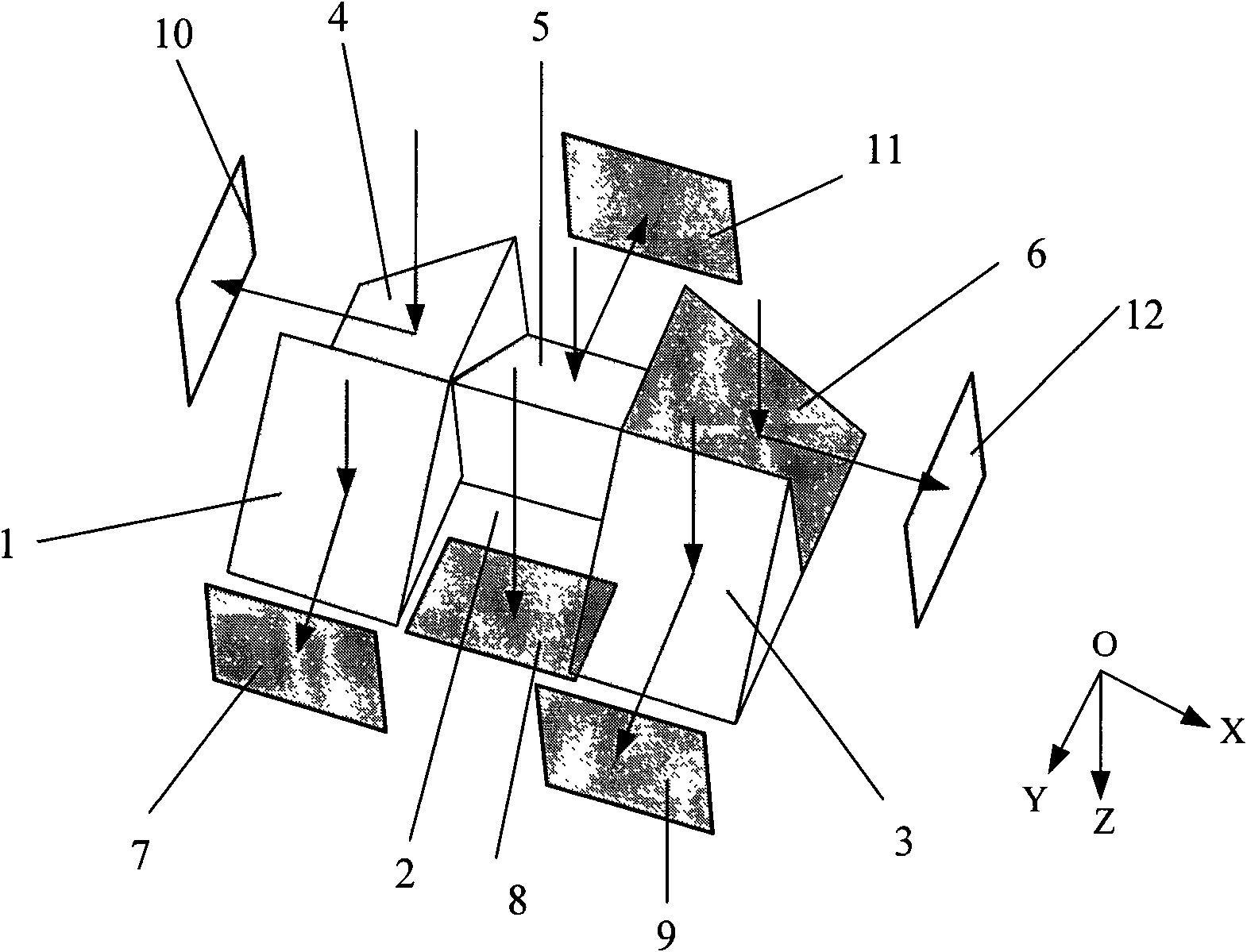
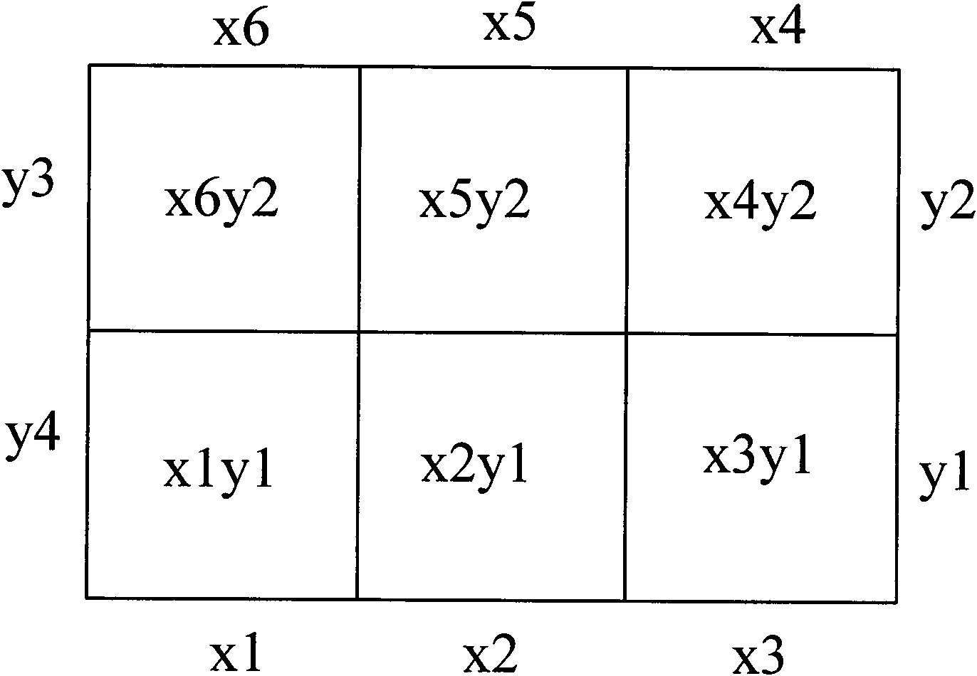
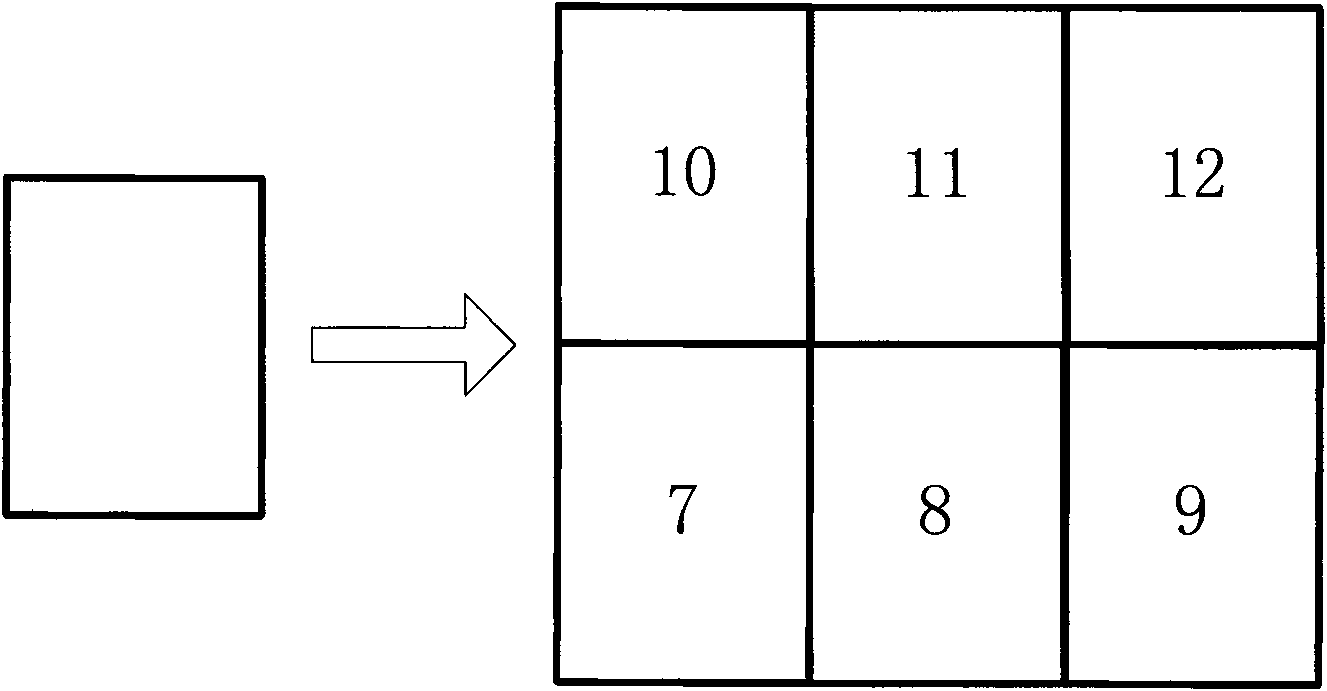
[0030] like figure 1 As shown, it is a splicing schematic diagram for realizing the splicing of 6 small-area array devices into a 2×3 mode large-area array device. For the convenience of description, a space rectangular coordinate system should be established first. The coordinate system takes the light propagation direction as the positive direction of the Z-axis (here, the vertical downward direction is selected), the positive direction of the Y-axis when the vertical paper faces outward, and the positive direction of the X-axis by the right hand. The rule is determined, the coordinate origin is O.

[0031] Six identical detectors are placed in sequence in spatial positions. The planes where the first detector 7 , the third detector 9 and the fifth detector 11 are located are all parallel to the XOZ plane, and the first detector 7 and the third detector 9 are located on the plane. The plane intersects the positive half-axis of the Y-axis, the plane where the fifth detector ...


PUM


Abstract

Along with the further improvement of requirements of large-size array photoelectric devices, the research of the splicing technology of array photoelectric devices needs to be developed urgently. Theinvention relates to an optical splicing method of a large-array photoelectric device, which achieves a condition that six small-array devices are spliced into a large-array device with a 2*3 mode, or four small-array devices are spliced into a large-array device with a 2*2 mode by adopting prism-type splicing and adjusting the positions of a prism and the array devices in space; and the splicingmethod is simple and easy for engineering realization, and can satisfy the requirements to large-array photoelectric detectors in the space remote sensing field.

Description

technical field [0001] The invention belongs to the technical field of aerospace optical remote sensors, and relates to a method for optical splicing of large-area array photoelectric devices applied to a space remote sensor. Background technique [0002] With the development of space remote sensors, the demand for large-scale area array photoelectric detection devices is increasing day by day, such as geostationary orbit staring satellite remote sensors, low-orbit frame digital surveying and mapping remote sensors, aerial frame digital remote sensors, cryogenic optical ultra-large-scale remote sensors Matrix cosmic space thermal vision instrument, deep space exploration and space experiment technology, etc. Large area array photoelectric detection remote sensor is an important direction for the development of my country's space remote sensor in the future, and an important means to improve the temporal resolution of optical remote sensing in my country. [0003] Due to the...

Claims


Application Information

Patent Timeline
Patent Type & Authority Applications(China)
IPC IPC(8): G01S7/481G02B5/04
Inventor 兰丽艳阮宁娟李妥妥马建华郭悦林宏宇
Owner BEIJING RES INST OF SPATIAL MECHANICAL & ELECTRICAL TECH
Why Eureka
Try Eureka