Defect test structure of semiconductor device, defect test method and defect test structure of before-metal medium layer

A defect testing, semiconductor technology, applied in the direction of semiconductor/solid-state device testing/measurement, semiconductor devices, semiconductor/solid-state device components, etc., can solve the problems of device short circuit, reduced efficiency, expensive, etc., to reduce costs and save test steps , the effect of improving production efficiency

Inactive Publication Date: 2010-02-17
SEMICONDUCTOR MANUFACTURING INTERNATIONAL (BEIJING) CORP
View PDF1 Cites 5 Cited by
  • Summary
  • Abstract
  • Description
  • Claims
  • Application Information

AI Technical Summary

Problems solved by technology

figure 2 for figure 1 The enlarged cross-sectional schematic diagram along the D-D direction, the gate 30 (see figure 1 ) between the pre-metal dielectric layer 50 has a strip-shaped void defect 70, but in the actual production process, the pre-metal dielectric layer 50 is formed first, and then the contact hole 80 and the contact hole 90 are etched, respectively in the contact hole 80 and the contact hole. The hole 90 is filled with metal to form the metal contact plugs A1 and A2, and the void defect 70 conn

Method used


Image

  • Defect test structure of semiconductor device, defect test method and defect test structure of before-metal medium layer
  • Defect test structure of semiconductor device, defect test method and defect test structure of before-metal medium layer
  • Defect test structure of semiconductor device, defect test method and defect test structure of before-metal medium layer

Examples


Embodiment 1

[0071] In this embodiment, the detection of void defects in the pre-metal dielectric layer is taken as an example, combined with the attached Figure 4 to Figure 7 A defect test structure and a defect test method of a semiconductor device are described in detail.

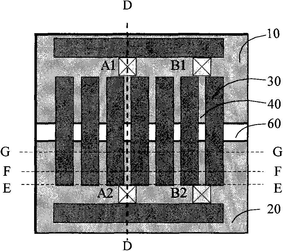
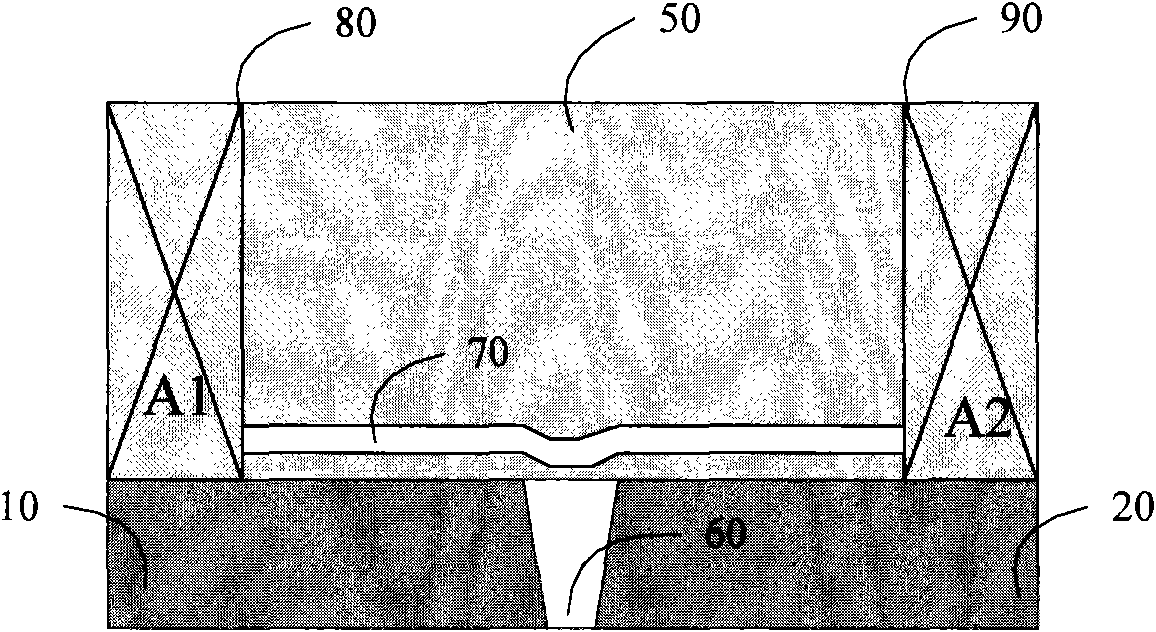
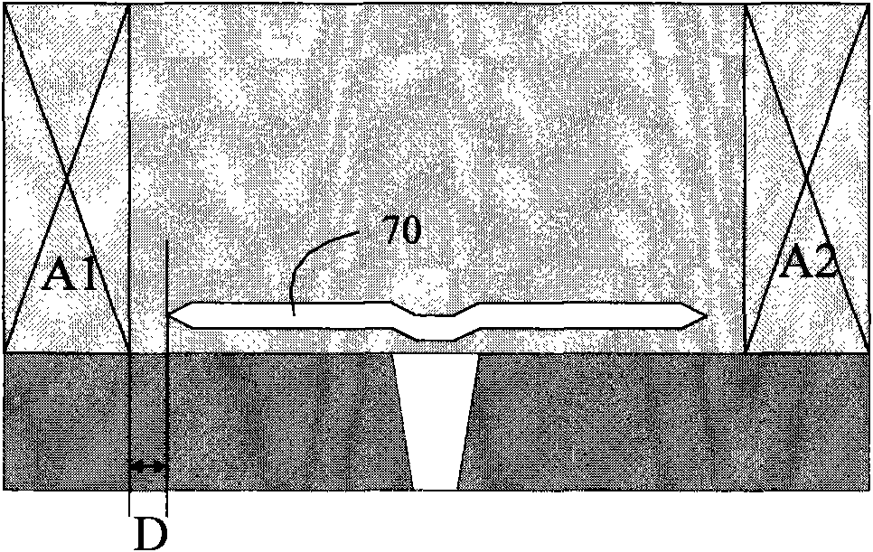
[0072] In this embodiment, the defect testing structure of the semiconductor device is used to test void defects in the pre-metal dielectric layer, and the defect testing structure of the semiconductor device is the defect testing structure of the pre-metal dielectric layer. Figure 4 It is a top view of the defect test structure of the pre-metal dielectric layer, the defect test structure includes: a semiconductor substrate (not shown in the figure), an active region 110 and an active region 120 on the substrate, and the active region 110 and the shallow trench isolation region 130 between the active region 120, the active region 110 and 24 parallel gates 140 above the active region 120, and the 23 parallel gates 1...

Embodiment 2

[0088] This embodiment takes testing the void defect in the shallow trench isolation region as an example, combined with the attached Figure 8 to Figure 9 The defect testing structure and defect testing method of the semiconductor device are described in detail.

[0089] Figure 8 It is a top view of the defect test structure of the shallow trench isolation region, and the defect test structure includes: a semiconductor substrate (not shown in the figure), an active region 210 on the substrate, and a shallow trench for isolating the insulating active region 210 a trench isolation region 260, the shallow trench isolation region 260 is filled in the corresponding trench 250, Figure 8 The six grooves 250 shown in the figure are arranged in parallel with each other, and the connection line A'-A' at one end of the six grooves 250 intersects the vertical direction B'-B' of the grooves 250, and the included angle is greater than 0 degrees and less than An acute angle of 90 degree...


PUM

PropertyMeasurementUnit
Angleaaaaaaaaaa

Abstract

The invention discloses a defect test structure of a semiconductor device, a defect test method and a defect test structure of a before-metal medium layer, wherein the defect test structure of the semiconductor device comprises a semiconductor substrate, n grooves which are arranged on the semiconductor substrate and parallel to one another, and a medium layer filled in the grooves; n is a naturalnumber which is more than or equal to 3; and in a top view of the defect test structure, an inclination angle between a connecting line connecting one end of all grooves and a vertical line of the grooves is beta. Correspondingly, the invention also discloses the defect test method of the semiconductor device and the defect test structure of the before-metal medium layer. The defect test structure and the defect test method have the advantages of saving test steps, improving production efficiency, and facilitating cost reduction.

Description

technical field [0001] The invention relates to the technical field of semiconductor manufacturing, in particular to a defect testing structure of a semiconductor device, a defect testing method and a defect testing structure of a pre-metal dielectric layer. Background technique [0002] With the increasing demand for high integration and high performance of ultra-large-scale integrated circuits, semiconductor technology is developing towards technology nodes with 65nm or even smaller feature sizes. With the continuous scaling down of device sizes, gap filling capabilities of thin film deposition are also required (Gap-fill ability) has been further improved. For example, the High Density Plasma PhosphoSilicate Grass (HDPPSG) process used to form the pre-metal dielectric layer (Pre-Metal Dielectric, PMD) has been proven to be used in the manufacture of logic circuits at the 90nm technology node. The pre-metal dielectric layer filled in the window between the gate structures...

Claims


Application Information

Patent Timeline
IPC IPC(8): H01L23/544H01L21/66
Inventor 郑春生刘明源张文广
Owner SEMICONDUCTOR MANUFACTURING INTERNATIONAL (BEIJING) CORP
Why Eureka
Try Eureka