

Multi-element doping n-type zinc-oxide-base transparent conducting film and preparation method thereof
A transparent conductive film, zinc oxide-based technology, applied in metal material coating process, vacuum evaporation plating, coating and other directions, can solve problems such as performance degradation, poor stability of ZnO-based film, and inability to meet solar cell applications. , to achieve the effect of improving stability, easy quality monitoring, and improving stability
- Summary
- Abstract
- Description
- Claims
- Application Information
AI Technical Summary
Problems solved by technology
Method used
Image

Examples
Embodiment 1
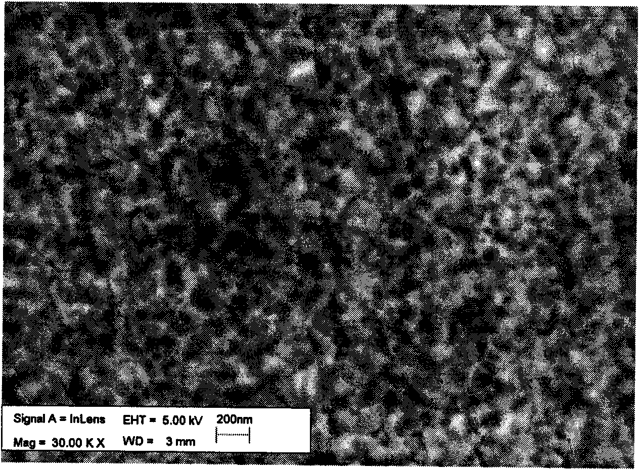
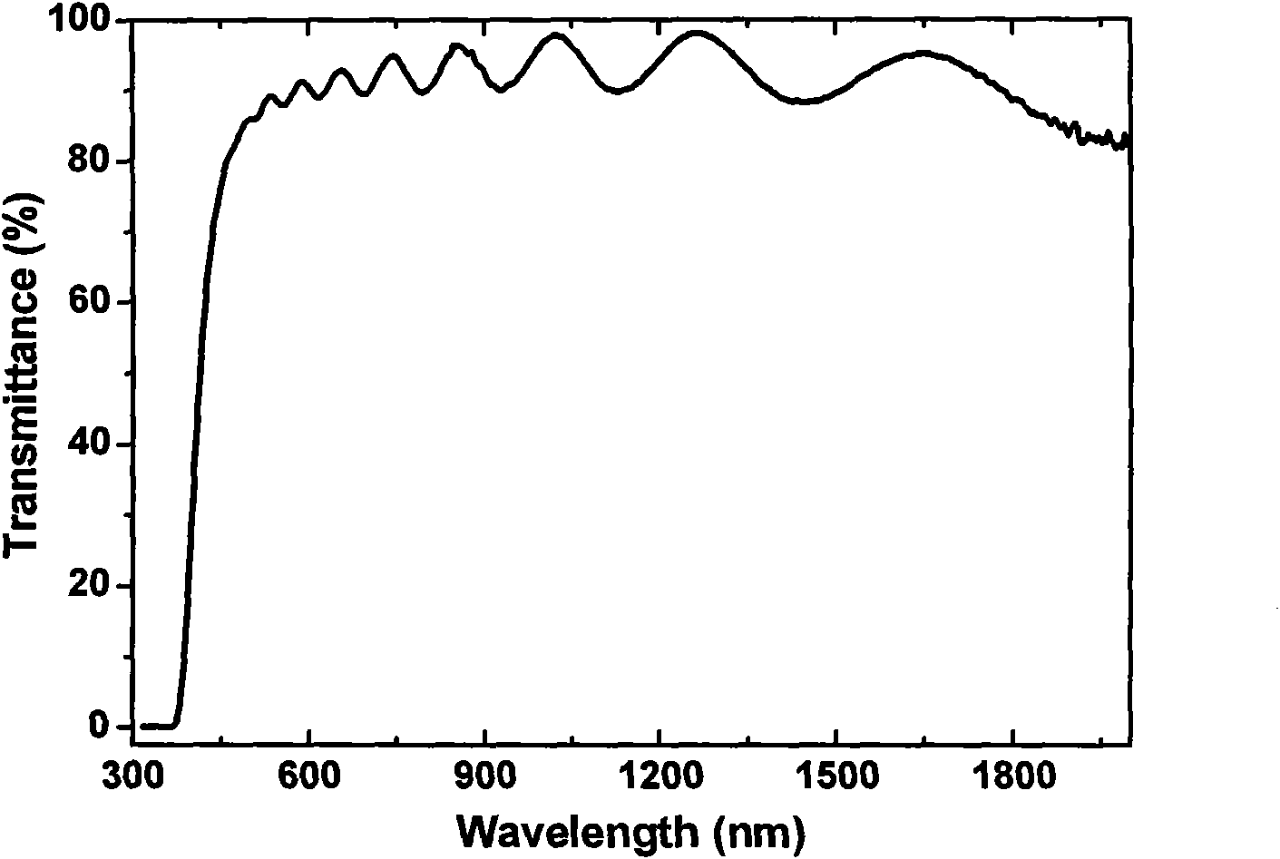
[0039] Using ZnO-based doping compound (ZnO:Al, Si) as the target material, the doping ratios of Al and Si are 2.0mol% and 3.0mol%, respectively, and ordinary glass is used as the substrate, and the background vacuum is pumped to 2.0×10 -4 Pa, with high-purity argon as the working gas, and a small amount of O 2 and H 2 Gas (O 2 and H 2 accounted for 3% and 6% of the total gas flow respectively), the working pressure was maintained at 1.0Pa, the substrate temperature was 150°C, the distance between the target and the substrate was set at 7.5cm, DC magnetron sputtering was adopted, and the sputtering power was 80W , the deposition time is 40min. The film has a visible light transmittance of 88% and an electronic conductivity of 1.5×10 4 S / cm, the retention rate of electrical conductivity and light transmittance is above 98% after accelerated aging for 50 hours in an environment with a temperature of 60 degrees Celsius and a relative humidity of 70%. The SEM images, transmis...
Embodiment 2
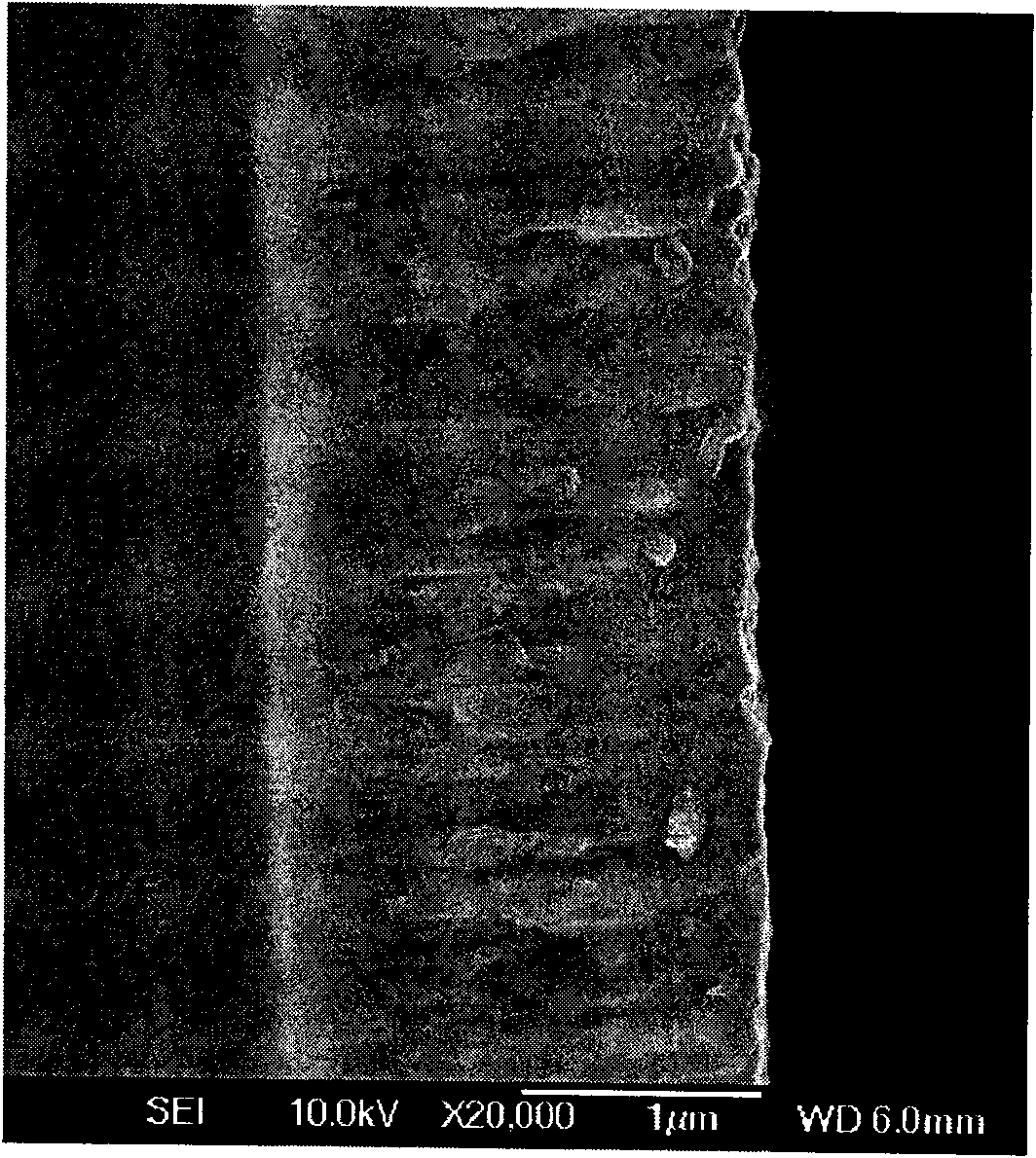
[0042] Using ZnO-based doping compound (ZnO:Al, Sn) as the target material, the doping ratio of Al and Sn is 2.0mol% and 5mol%, and using ordinary glass as the substrate, the background vacuum is pumped to 2.0×10 -4 Pa, with high-purity argon as the working gas, the working pressure is maintained at 1.2Pa, the substrate temperature is 150°C, the distance between the target and the substrate is set at 7cm, DC magnetron sputtering is used, the sputtering power is 120W, the deposition time After 40 min, the crystal grains grew obviously, and the crystalline quality of the film was significantly improved. The thickness of the film is about 1500nm, the transmittance of visible light is above 85%, and the electronic conductivity is 1.2×10 4 S / cm, the retention rate of electrical conductivity and light transmittance is above 90% after accelerated aging for 50 hours in an environment with a temperature of 60 degrees Celsius and a relative humidity of 70%.
Embodiment 3
[0044] Using ZnO-based doping compound (ZnO:Al, In) as the target material, the doping ratio of Al and In is 2.0mol% and 5mol%, and using ordinary glass as the substrate, the background vacuum is pumped to 2.0×10 -4 Pa, with high-purity argon as the working gas, and a small amount of O 2 and H 2 Gas (O 2 and H 2 accounted for 5% and 2% of the total gas flow respectively), the working pressure was maintained at 1.2Pa, the substrate temperature was 90°C, the distance between the target and the substrate was set at 7cm, radio frequency magnetron sputtering was used, and the sputtering power was 60W. The deposition time is 30min. Next, adjust O 2 and H 2 Gas volume (O 2 and H 2 accounted for 0.05% and 5.0% of the total gas flow respectively), the working pressure was maintained at 0.3Pa, the substrate temperature was room temperature, the distance between the target and the substrate was set at 5cm, DC magnetron sputtering was adopted, and the sputtering power was 140W. Th...
PUM
| Property | Measurement | Unit |
|---|---|---|
| Mobility | aaaaa | aaaaa |
| Conductivity | aaaaa | aaaaa |
| Conductivity | aaaaa | aaaaa |
Abstract
Description
Claims
Application Information