Method for realizing continuous gluing of semiconductor wafer and purification system thereof

A purification system and semi-conductor technology, which is applied to the surface coating liquid device, coating, photoplate making process coating equipment, etc., can solve the problems of blocking and polluting the purification room, so as to reduce the workload and save costs , work smoothly

Active Publication Date: 2010-03-10
LATTICE POWER (JIANGXI) CORP
View PDF6 Cites 0 Cited by
  • Summary
  • Abstract
  • Description
  • Claims
  • Application Information

AI Technical Summary

Problems solved by technology

[0009] Since the purification room is an ash-free space, it is generally not allowed to use cotton balls. However, cotton balls must be used in the above method of cleaning the disk protection. pollution clean room;
[0010] Both photoresist and acetone are toxic items, especially acetone is very volatile. Even if there is a ventilation system to purify the air in the purification room, the damage to the human body from the toxic gas will continue during the entire cleaning process of the protective plate. Therefore, it is necessary to Further improve the working environment for staff
In addition, due to the laying of foot pads on the floor, a large number of foot pads around the glue applicator prevent the circulation of indoor air

Method used


Image

  • Method for realizing continuous gluing of semiconductor wafer and purification system thereof
  • Method for realizing continuous gluing of semiconductor wafer and purification system thereof
  • Method for realizing continuous gluing of semiconductor wafer and purification system thereof

Examples


Embodiment Construction

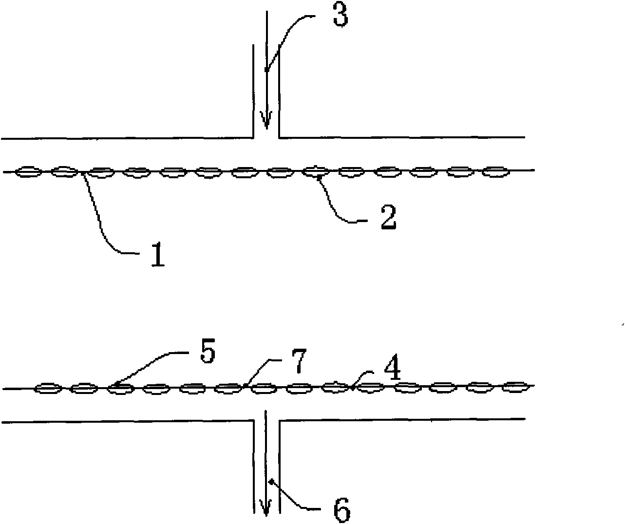
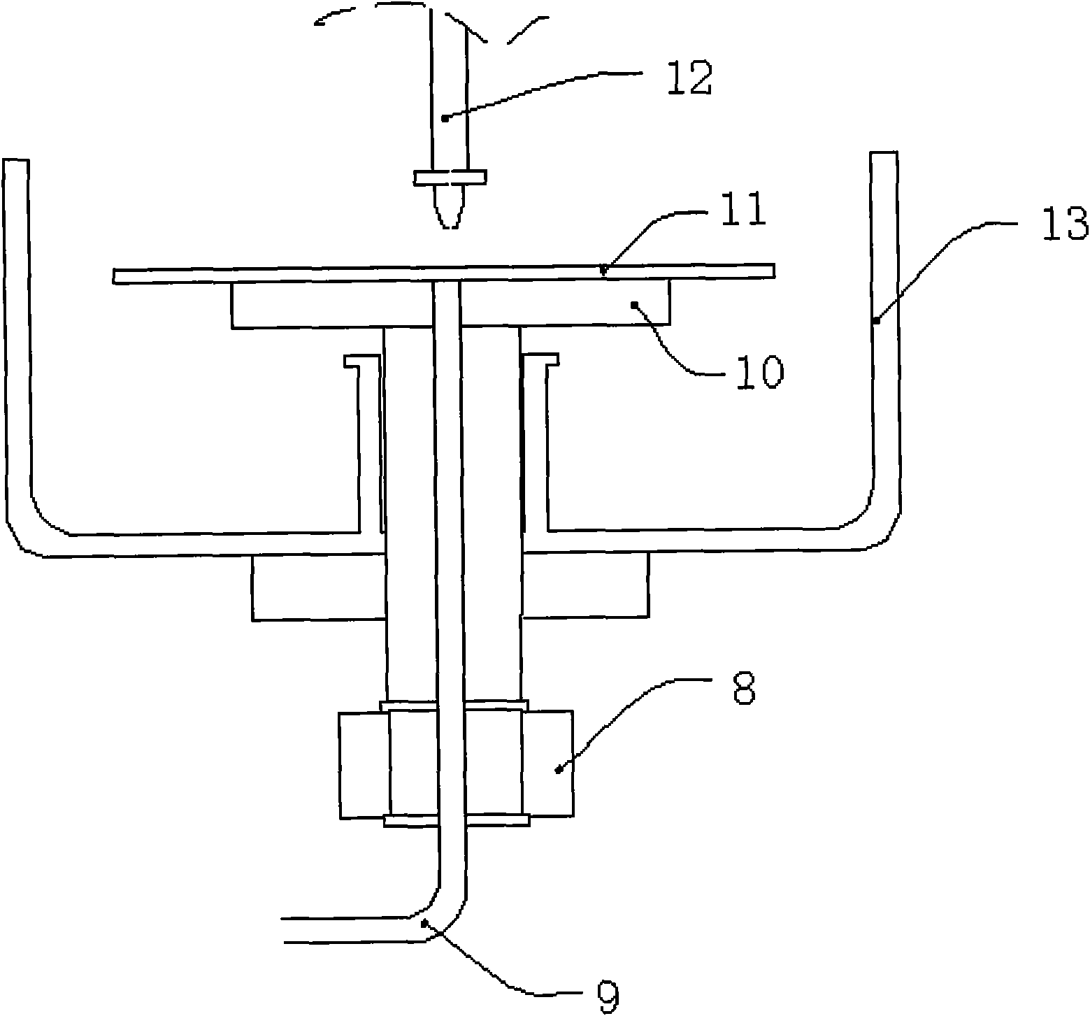
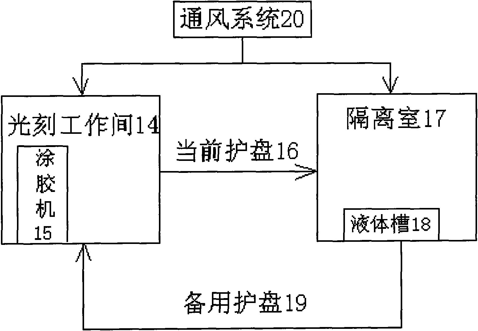
[0033] The invention provides a purification system for realizing continuous coating of semiconductor wafers. For its structural principle, see image 3 . The purification system includes a photolithography booth 14 , a glue applicator 15 , a ventilation system 20 , an isolation chamber 17 , a liquid tank 18 and a spare protection plate 19 . Wherein the ventilation site is the isolation room 17, of course the ventilation site can also be an outdoor natural environment.

[0034] The glue applicator 15 is placed on the grid-shaped anti-corrosion floor in the photolithography workshop 14 . The gluing machine includes a current backing plate (that is, a backing plate to be cleaned on the gluing machine) 16 . The current protection plate 16 is sent into the liquid tank 18 in the isolation chamber 17 for soaking. After a period of time, take out the current backing plate 16 and dry it, make the organic solvent on the top of the backing plate volatilize and take it back to the li...


PUM


Abstract

The invention provides a method for realizing the continuous gluing of a semiconductor wafer and a purification system thereof, which are used for improving the efficiency of semiconductor gluing, simultaneously purifying air in a working room, improving the indoor air of the gluing working room and being conductive to physical and psychological health of working staff. The technology mainly comprises the following steps: gluing is carried out on the semiconductor wafer; removing a first protective disc filled with waste glue when the waste glue in the protective disc on the gluing machine is accumulated to a certain extent and needs to be cleared up; placing the first protective disc filled with the waste glue into a liquid trough filled with an organic solvent, using the organic solvent for soaking the first protective disc, removing after the dissolution of the waste glue for standby after the complete volatilization of the organic solvent, and arranging the liquid trough in a ventilation place which is isolated with the working room; and simultaneously mounting a second protective disc for standby after the completion of the clearing up on the gluing machine while removing the first protective disc filled with the waste glue. The method and the purification system are mainly used for the gluing technology before the semiconductor lithography.

Description

technical field [0001] The invention relates to the manufacture of semiconductors, in particular to the clean and environment-friendly technology of photoresist coating of semiconductors. Background technique [0002] In the process of manufacturing semiconductor epitaxial wafers, multiple processes will involve the process of photolithography many times, taking the manufacture of LED epitaxial wafers with silicon growth substrates as an example. Grooving on the growing silicon substrate, making complementary P electrodes, making adhesive layers, edge removal, passivation, and making P electrodes all require photolithography. Before photolithography, the film needs to be coated with a mask. And glue mask must use glue machine. The coating machine can evenly coat the photoresist on the film. [0003] Since the production of semiconductor epitaxial wafers is now completed in a high-purity purification room, the purification room is a closed space isolated from the outside wo...

Claims


Application Information

Patent Timeline
Patent Type & Authority Applications(China)
IPC IPC(8): B05C21/00G03F7/16
Inventor 邹灵威
Owner LATTICE POWER (JIANGXI) CORP
Why Eureka
Try Eureka