Processing method of gap filling and manufacturing method of shallow trench isolation groove

A processing method and gap filling technology, which is used in semiconductor/solid-state device manufacturing, electrical components, circuits, etc., can solve the problems of reduced film performance, poor uniformity, and increased etching rate, so as to improve performance and avoid performance. The effect of reducing and improving film properties

Inactive Publication Date: 2010-03-17
SEMICONDUCTOR MANUFACTURING INTERNATIONAL (BEIJING) CORP
View PDF1 Cites 8 Cited by
  • Summary
  • Abstract
  • Description
  • Claims
  • Application Information

AI Technical Summary

Problems solved by technology

[0013] The above hydrogen passivation method can effectively remove F element, but the H2 used to remove F element will still have after the reaction Part remains in the chamber and enters the generated STI film in the subsequent gap-fill operation
h 2 After entering the STI film, many performance parameters of the film will be reduced: for example, the density of the STI film will decrease, the uniformity will deteriorate, and the etching rate will increase, which

Method used


Image

  • Processing method of gap filling and manufacturing method of shallow trench isolation groove
  • Processing method of gap filling and manufacturing method of shallow trench isolation groove
  • Processing method of gap filling and manufacturing method of shallow trench isolation groove

Examples


Embodiment Construction

[0038] In order to make the object, technical solution and advantages of the present invention clearer, the present invention will be further described in detail below with reference to the accompanying drawings and examples.

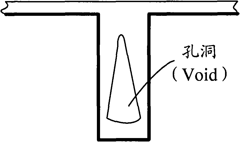
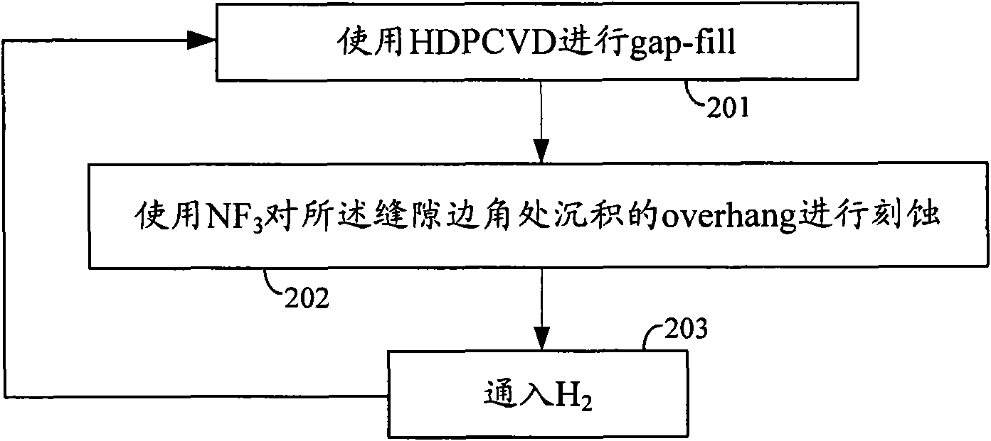
[0039] An embodiment of the present invention provides a gap filling processing method, which is used to form a thin film on a semiconductor substrate with a gap and completely fill the gap. The process is as follows image 3 shown, including:

[0040] Step 301: use HDPCVD to perform gap-fill;

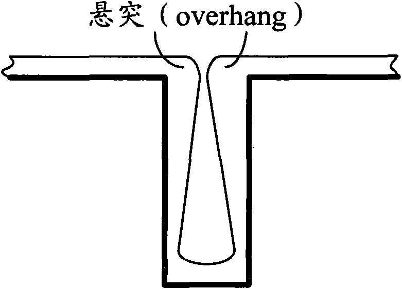
[0041] Step 302: use NF 3 Etching (etch) the overhang deposited at the corners of the slit to prevent it from sealing the opening of the slit;

[0042] Step 303: After the first etching is completed, inject H 2 carry out hydrogen passivation treatment;

[0043] Step 304: Introduce oxygen to react with the residual hydrogen gas after the hydrogen passivation treatment, and discharge the remaining gas out of the reaction chamber, and return to step 301 until t...


PUM


Abstract

The invention discloses a processing method of gap filling, which is used for forming a thin film on a semiconductor substrate with a gap and completely filling the gap. The processing method comprises the following steps: using a method of high-density plasma chemical vapor deposition (PCVD) to fill the gap; using nitrogen trifluoride to etch the overhang deposited in the corner of the gap; afterintroducing hydrogen gas for hydrogen passivating treatment, introducing oxygen gas to react with the residual hydrogen gas after hydrogen passivating treatment, and discharging all the gases in thereaction chamber; and then, returning to carry out the gap filling operation until the filling of the gap is completed. The embodiment of the processing method of gap filling can remove the residual hydrogen gas in the reaction chamber by introducing the oxygen gas after the hydrogen passivating treatment so as to prevent the hydrogen gas from being introduced into the generated thin film, avoid various kinds of performance reduction caused by the generation of H2 and improve the performance of the thin film. The invention also discloses a manufacturing method of a shallow trench isolation groove, which can improve the performance of an isolation groove thin film.

Description

technical field [0001] The invention relates to integrated circuit manufacturing technology, in particular to a gap filling processing method and a shallow trench isolation groove manufacturing method. Background technique [0002] At present, integrated circuit technology has entered the era of ultra-large-scale integrated circuits. As the process size of integrated circuits develops to 65 nanometers or even finer structures, the aspect ratio (that is, the ratio of the depth of the gap to the width of the gap) in some devices has reached 4:1 or even higher. In this case, higher technological requirements are put forward for the filling of various gaps, especially the filling of gaps with high aspect ratios. [0003] Chemical vapor deposition (Chemical Vapor Deposition, CVD) is able to deposit a film (Film) on a semiconductor substrate by means of a chemical gas reaction, thus filling the gap (usually referred to as gap filling, or gap-fill) It has been widely used in the ...

Claims


Application Information

Patent Timeline
IPC IPC(8): H01L21/00H01L21/762
Inventor 胡亚威刘明源郑春生
Owner SEMICONDUCTOR MANUFACTURING INTERNATIONAL (BEIJING) CORP
Why Eureka
Try Eureka