

Structure taking part of metal grid as grid medium etching blocking layer with high dielectric constant and integration method
A technology for etching barrier layers and high dielectric constants, which is applied in the manufacture of circuits, electrical components, semiconductors/solid-state devices, etc., can solve problems such as damage to high-K gate dielectric materials, simplify integration complexity, and overcome Fermi The effect of the energy level pinning effect
- Summary
- Abstract
- Description
- Claims
- Application Information
AI Technical Summary
Problems solved by technology
Method used
Image

Examples
Embodiment Construction
[0027] Below in conjunction with accompanying drawing and specific embodiment the present invention is described in further detail:
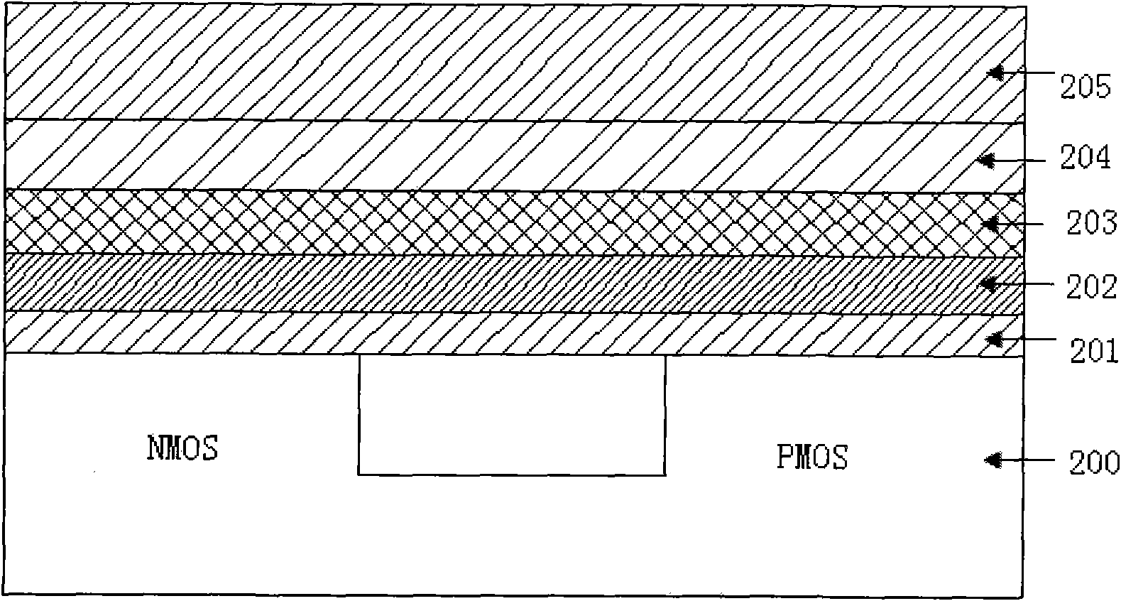
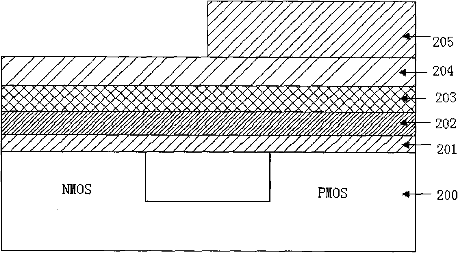
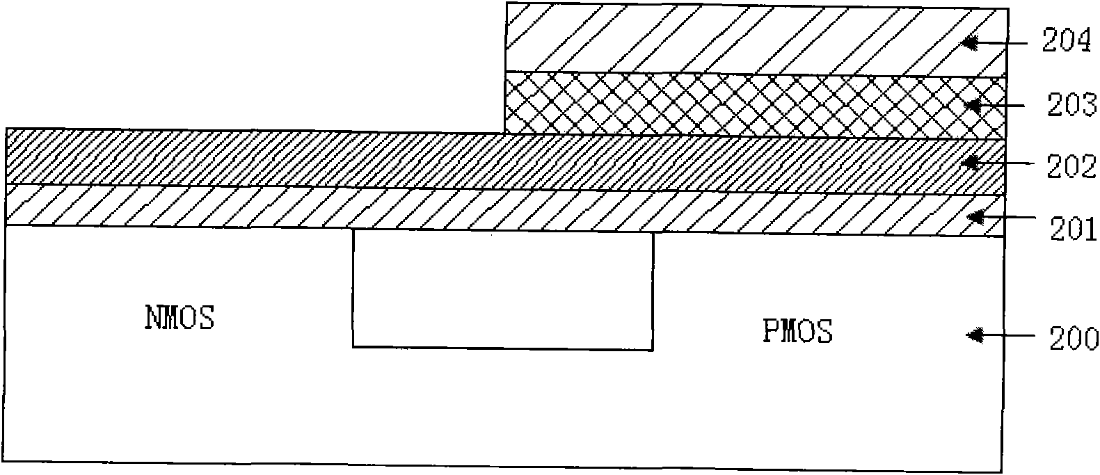
[0028] Step 1: Please refer to figure 1 , provide a silicon substrate 200 that has completed the shallow trench isolation (STI) process, and sequentially form a layer of film 201, a layer of film 202, a layer of film 203, a layer of film 204 and a layer of film 200 on the silicon substrate 200 Film 205. Thin film 201 is SiO 2 , with a thickness in the range of 1 to 5 nm. The thin film 202 and the thin film 203 are high-k dielectric layers, and the thin film 202 is HfSiO. Thin film 203 is Al 2 o 3 , the thin film 204 is TiN or WN, its thickness is in the range of 1 to 10 nanometers, and it is an etching barrier layer. The thin film 205 is a photoresist layer, and the thickness of the photoresist is in the range of 0.3 to 2 microns. After the thin film 202 and the thin film 203 are formed, an annealing treatment is required before the thin...
PUM
 Abstract
Description
Claims
Application Information