Panel and manufacturing method thereof

A manufacturing method and panel technology, which can be used in instruments, nonlinear optics, optics, etc., and can solve problems such as defects

Active Publication Date: 2012-02-29
K TRONICS (SUZHOU) TECH CO LTD +1
View PDF3 Cites 1 Cited by
  • Summary
  • Abstract
  • Description
  • Claims
  • Application Information

AI Technical Summary

Problems solved by technology

[0004]However, the inventor found in the process of implementing the above technical solution: in the current structure of the sealant, since gold balls are doped in all the sealants, It will inevitably bring about two major disadvantages: one is that in the area of ​​the data line lead (Fan out) 101 corresponding to the data line pad (Data Pad) 104, it will cause multiple occurrences of electrostatic discharge (ESD), such as Figure 2 shows the corresponding pads of the data lines in the existing sealant structure Schematic diagram of the area of ​​the data line lead, where the data line pad 104 is located on the array substrate 103, due to the existence of gold balls, it will cause a short circuit between the data line lead 101 and the common electrode 113 on the color filter substrate 102, thus causing the corresponding line to be defective ESD usually occurs at E in Figure 3 point, Figure 3 is the structure of the existing sealing glue A cross-sectional view along position A-A in Figure 2, in addition, From Figure 2, you can also see the sealing glue 105 The positional relationship with the black matrix (BM) 106; the second is that all the sealants are doped with gold balls, so the use of gold balls is relatively large, which increases the cost of the LCD panel to a certain extent; The third is that the inventors also found that the occurrence of defective lines has nothing to do with the density of gold balls doped in the sealant, which means that reducing the doping density cannot fundamentally solve the problem, so a new sealant structure is needed to solve the problem. Solve the bad line caused by the use of golden ball

Method used


Image

  • Panel and manufacturing method thereof
  • Panel and manufacturing method thereof
  • Panel and manufacturing method thereof

Examples


Embodiment Construction

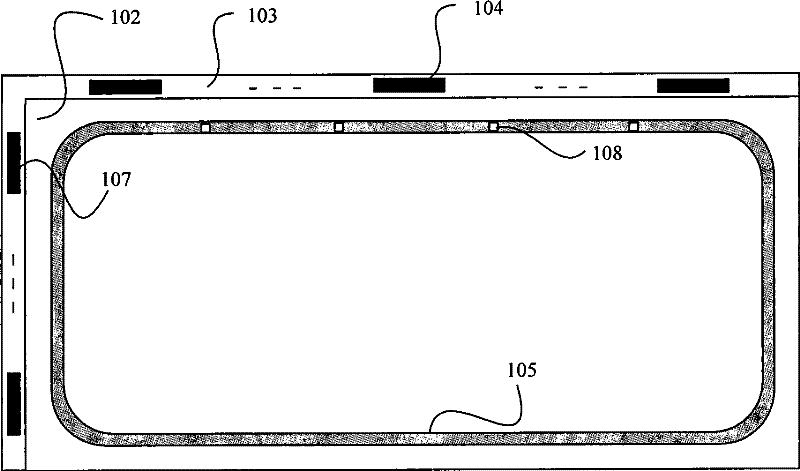
[0030] Such as Figure 4 As shown, it is a structural schematic diagram of an embodiment of the sealing glue of the present invention. The secondary sealing glue 2 is doped with a certain density of gold balls, as long as it is selectively coated in a dot shape, and its coating position is generally the main sealing frame. The outer side of the adhesive 1, and can be selected on the four peripheries of the array substrate 103, such as the side with the data line pad 104, the side with the gate line pad 107, the side opposite the data line pad 104, and the gate line pad. On the opposite side of the disk 107, it is usually selected in the middle of the data line pad on the side with the data line pad 104, as shown in the figure; in order to better avoid the occurrence of ESD, the secondary sealing glue 2 needs to be Avoid the data line lead area, preferably also avoid the gate line lead area.

[0031] Such as Figure 5 Shown is a flowchart of an embodiment of the panel manufac...


PUM

PropertyMeasurementUnit
diameteraaaaaaaaaa
widthaaaaaaaaaa

Abstract

The invention relates to a panel and a manufacturing method thereof, wherein, the manufacturing method of the panel comprises the following steps: finishing the manufacturing of film transistor arrays and peripheral graphs on a substrate to form an array substrate; coating main frame sealing glue in which no golden ball is doped at the periphery of the array substrate; coating secondary frame sealing glue in which golden balls are doped outside of the main frame sealing glue, wherein the secondary frame sealing glue is partly overlapped with or completely separated from the main frame sealingglue, and is positioned in the connecting electrode area of the array substrate but keeps away from the lead wire area of data lines; and aligning the array substrate and a color-film substrate to form the panel. To the panel and the manufacturing method thereof, due to the absence of golden balls in the lead wire area of the date lines, ESD can not occur, simultaneously golden balls are only doped in the secondary frame sealing glue, the usage amount of golden balls is greatly reduced, thereby lowering the cost of the panel.

Description

technical field [0001] The invention relates to a panel and a manufacturing method of the panel, in particular to a panel with a main sealing frame glue and a secondary sealing frame glue structure and a manufacturing method thereof, belonging to the field of liquid crystal display manufacturing. Background technique [0002] In the field of flat panel display, thin film transistor (TFT) liquid crystal display (LCD) has gradually become the mainstream product in the field of flat panel display due to its advantages of light weight, thin thickness, no radiation, and low power consumption. In order to further improve the display quality and reliability of liquid crystal displays, various new manufacturing processes, new materials and new structures have been successfully developed, including the optimization of the structure of the sealant. The sealant 105 in the panel of the liquid crystal display is generally coated with Around the array (Array) substrate 103 or the color fi...

Claims


Application Information

Patent Timeline
Patent Type & Authority Patents(China)
IPC IPC(8): G02F1/1339G02F1/1333
Inventor 王章涛闵泰烨邱海军高文宝
Owner K TRONICS (SUZHOU) TECH CO LTD
Why Eureka
Try Eureka