
Method for adjusting response waveform of superconducting nano-wire photodetectors by utilizing buffer networks
A superconducting nanowire and buffer network technology, which is applied in the field of adjusting the response waveform of superconducting nanowire photodetectors, can solve the problems of increasing the complexity of the device manufacturing process and reducing the detection efficiency of the device, so as to reduce the falling edge time and improve Effect of Count Rate, Reduced Pulse Width
Patent Information
- Authority / Receiving Office
- CN · China
- Patent Type
- Patents(China)
- Current Assignee / Owner
- Publication Date
- 2011-04-27
- Estimated Expiration
- Not applicable · inactive patent
Smart Images
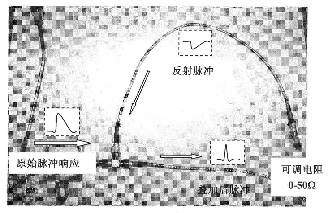
Figure 1 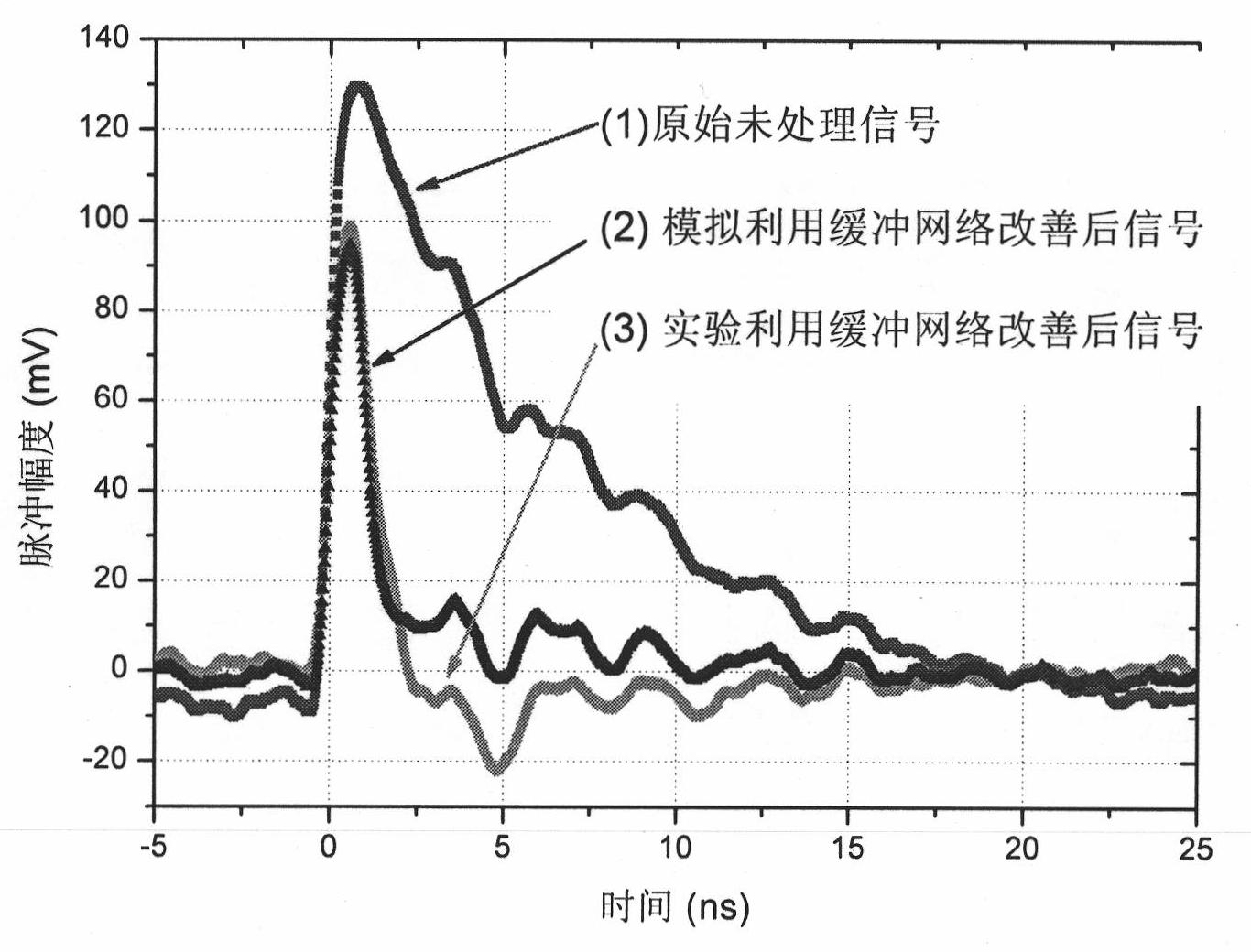
Figure 2 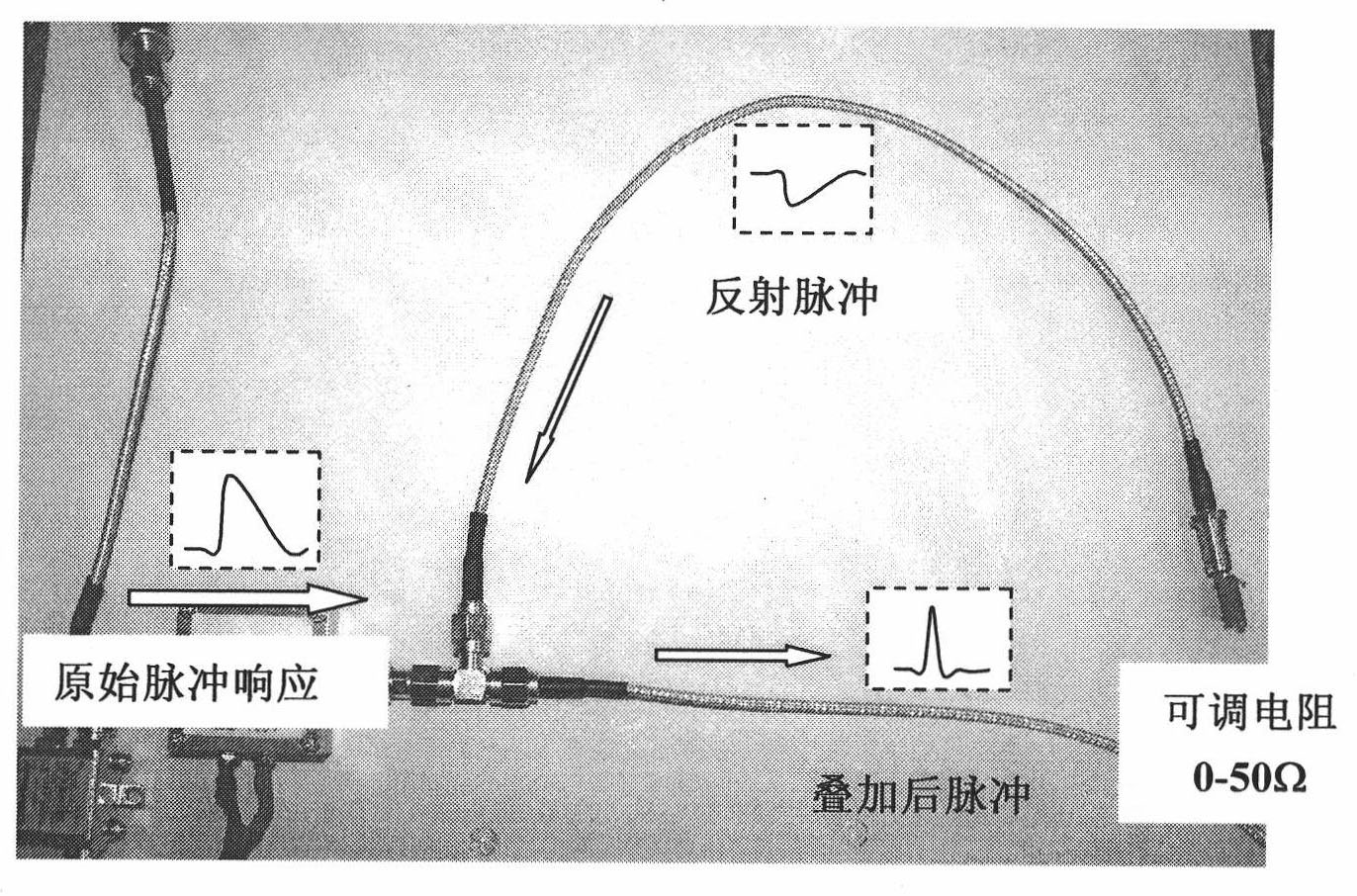
Figure 3
Abstract
Description
technical field
[0001] The invention relates to a method for adjusting the response waveform of a superconducting nanowire photodetector by using a buffer network. Background technique
[0002] Superconducting Nanowire Optical Detector (SNOD: Superconducting Nanowire Optical Detector) is a novel light detection method, which can be used for single photon detection with extreme sensitivity in the visible light to infrared band. SNOD devices mainly use low-temperature superconducting ultra-thin film materials, such as NbN, Nb, NbTiN, etc. The typical thickness is about 5 nanometers, and the device structure is usually a meandering nanowire structure with a width of about 100 nanometers [US2005051726A1].
[0003] Theoretically, the response time of a superconducting nanowire photodetector is determined by the thermal relaxation time of the material. For example, for a 3.5nm thick NbN film grown on a sapphire substrate, the thermal relaxation time is ~10 ps. [K.S.Ilin et al, ...
Examples
Embodiment 1
[0017] figure 1 As an implementation example: a typical coaxial cable RG174-U is used, the insulating material is cured polyethylene (Solid PE), and its electrical signal propagation velocity factor is f=0.66. Therefore, for a coaxial cable with a length of 10 cm, the time delay is about 1 ns. figure 2 It is the test and simulation results of the coaxial line length being 10cm and the adjustable resistance resistance of the termination being 0 ohms. The simulation and test results are basically consistent, making the pulse width at half maximum reduced from 4.5 nanoseconds to about 1.1 nanoseconds.
Embodiment 2
[0019] When the resistance value of the adjustable resistor is between 0 and 50 ohms, the pulse waveform will be between the waveform curve (1) and the curve (2). All the other are with embodiment 1.