
Method of producing large gate width silicon carbide metal semiconductor filed-effect transistor (SiC MESFET) with intercellular balance resistors

A technology for balancing resistors and manufacturing methods, applied in resistor manufacturing, resistors, circuits, etc., can solve problems such as low yield, difficult integration, and unstable device performance.

Active Publication Date: 2011-02-02
THE 13TH RES INST OF CHINA ELECTRONICS TECH GRP CORP
View PDF0 Cites 0 Cited by
  • Summary
  • Abstract
  • Description
  • Claims
  • Application Information

AI Technical Summary

Problems solved by technology

[0007] In view of the problems in the above-mentioned prior art that increasing the die gate width of semiconductor devices leads to unstable device performance, low yield, inability to effectively increase the output power of the device, or the introduction of power dividers and combiners, the production cost is high and the integration is difficult. The invention provides a method for manufacturing a large gate width SiC MESFET with an intercellular balance resistance that is simple to use and can effectively improve device stability and output power

Method used


Image

  • Method of producing large gate width silicon carbide metal semiconductor filed-effect transistor (SiC MESFET) with intercellular balance resistors
  • Method of producing large gate width silicon carbide metal semiconductor filed-effect transistor (SiC MESFET) with intercellular balance resistors
  • Method of producing large gate width silicon carbide metal semiconductor filed-effect transistor (SiC MESFET) with intercellular balance resistors

Examples


Embodiment Construction

[0023] In order to make the above objects, features and advantages of the present invention more obvious and understandable, the technical solutions in the embodiments of the present invention will be clearly and completely described below in conjunction with the drawings and specific implementation methods in the embodiments of the present invention. Obviously, The described embodiments are only some, not all, embodiments of the present invention. Based on the embodiments of the present invention, all other embodiments obtained by persons of ordinary skill in the art without making creative efforts belong to the protection scope of the present invention.

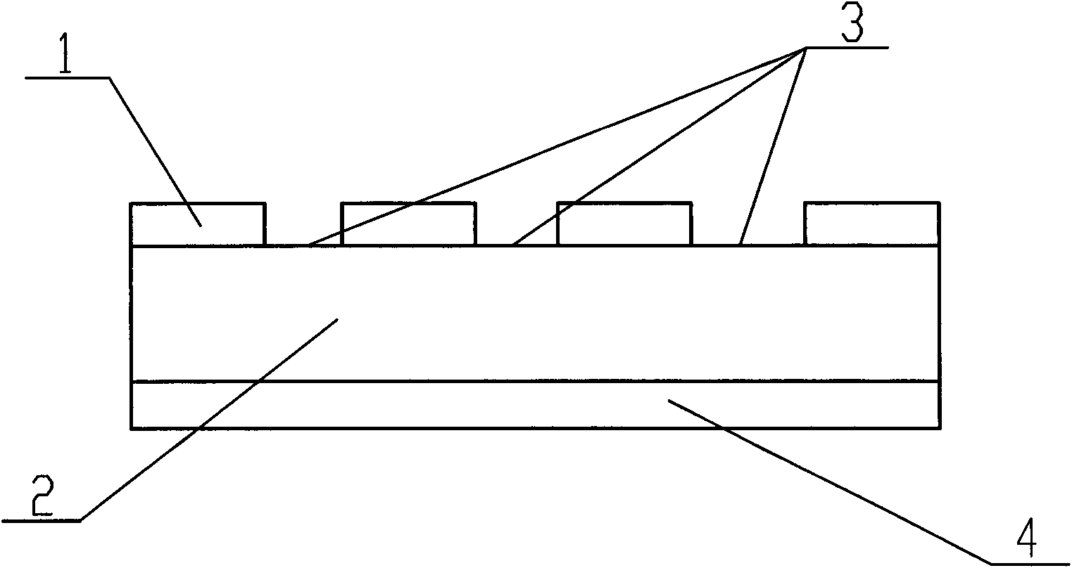
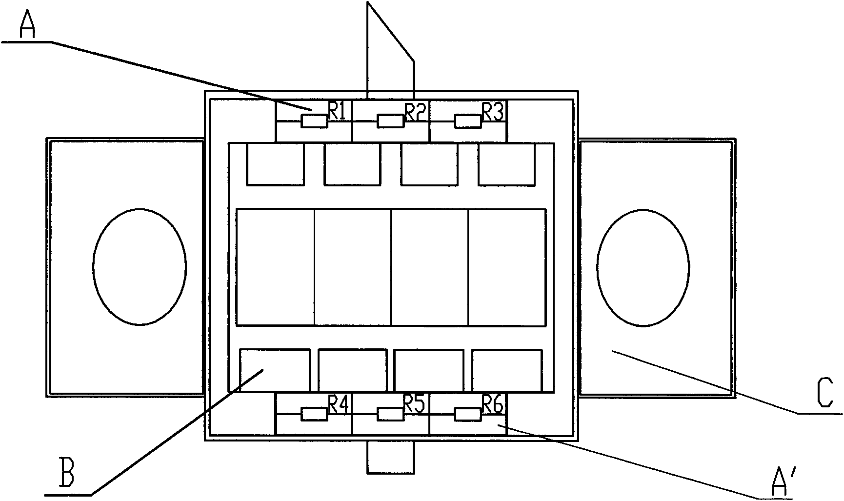
[0024] see figure 1 , The intercellular balance resistance structure described in the large gate width SiC MESFET with intercellular balance resistance includes a dielectric substrate 2 , a bonding wire bonding area 1 , a thin film resistance area 3 and a metal bottom layer 4 on the lower surface. The intercellular balance...


PUM


Abstract

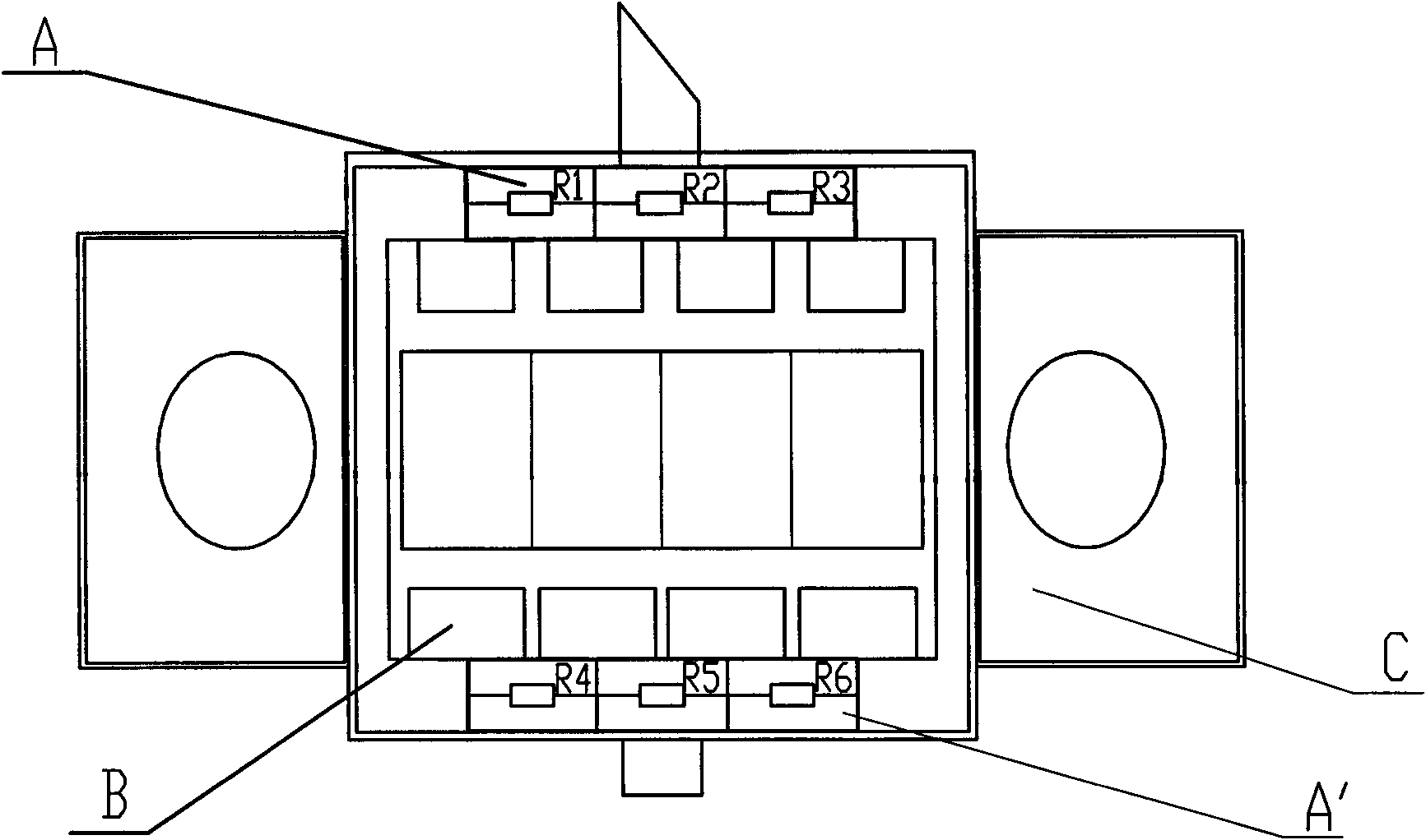
The invention relates to a method of producing a large gate width silicon carbide metal semiconductor filed-effect transistor (SiC MESFET) with intercellular balance resistors, mainly comprising the steps of additionally arranging the intercellular balance resistors in the process of producing the large gate width SiC MESFET and finally arranging one intercellular balance resistor on the input end of the large gate width SiC MESFET and one balance resistor on the output end of the large gate width SiC MESFET. The method of producing intercellular balance resistors is easy, and after the intercellular balance resistors are additionally arranged in the process of producing the large gate width SiC MESFET, the yield of the finished large gate width SiC MESFET can be improved, the large gate width SiC MESFET with stable performance and high reliability can be produced, and the output power of the large gate width SiC MESFET can be improved.

Description

technical field [0001] The present invention relates to the manufacture method of semiconductor device, specifically relate to the manufacture method of wide bandgap microwave semiconductor device SiC (silicon carbide, the same below) MESFET (metal semiconductor field effect transistor, the same below), more specifically, the present invention relates to Fabrication method of large gate width SiC MESFET with balanced resistance between them. Background technique [0002] Because of its excellent characteristics such as wide bandgap, high critical breakdown electric field, high thermal conductivity, and high carrier saturation drift velocity, SiC material has decided to apply it in the manufacture of semiconductor microwave power devices (especially MESFET). trend. At present, the research and development of power semiconductor devices is shifting from small power to high power. Today, there are two common methods for increasing the output power of semiconductor devices: ...

Claims


Application Information

Patent Timeline
Patent Type & Authority Patents(China)
IPC IPC(8): H01L21/50H01L21/48H01C17/00H01L21/60
CPCH01L2924/0002
Inventor 默江辉李亮王勇李静强冯震高学邦吴洪江
Owner THE 13TH RES INST OF CHINA ELECTRONICS TECH GRP CORP
Learn More