Method for detecting random defects of silicon gate of CMOS process

A defect and process technology, which is applied in the field of detecting random defects of CMOS process silicon gate, can solve problems such as increase, short circuit leakage, short circuit or open circuit, etc., and achieve the effect of improving process, increasing yield, and effectively utilizing test structure area

Inactive Publication Date: 2010-04-07
ZHEJIANG UNIV
View PDF0 Cites 4 Cited by
  • Summary
  • Abstract
  • Description
  • Claims
  • Application Information

AI Technical Summary

Problems solved by technology

When used as a transistor to control the gate, the defect of the silicon gate may lead to a short circuit between the source and drain of the transistor or an increase in leakage; when the silicon gate is connected to the upper metal through a via hole, the defect may cause an open circuit; cause short circuit or open circuit

Method used


Image

  • Method for detecting random defects of silicon gate of CMOS process
  • Method for detecting random defects of silicon gate of CMOS process
  • Method for detecting random defects of silicon gate of CMOS process

Examples


Embodiment Construction

[0027] The present invention will be described in detail below in conjunction with the accompanying drawings.

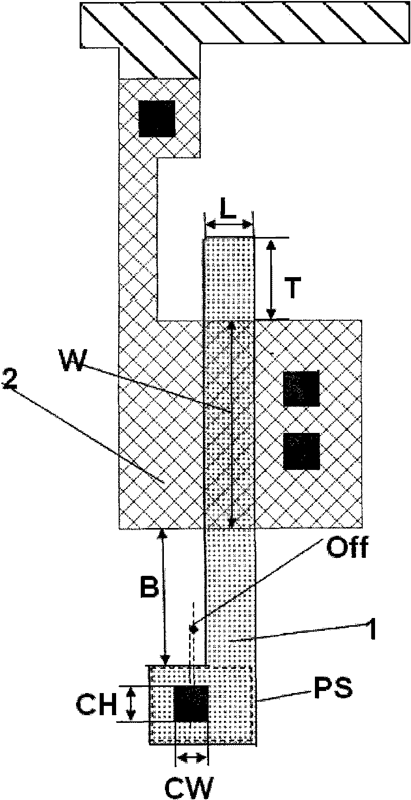
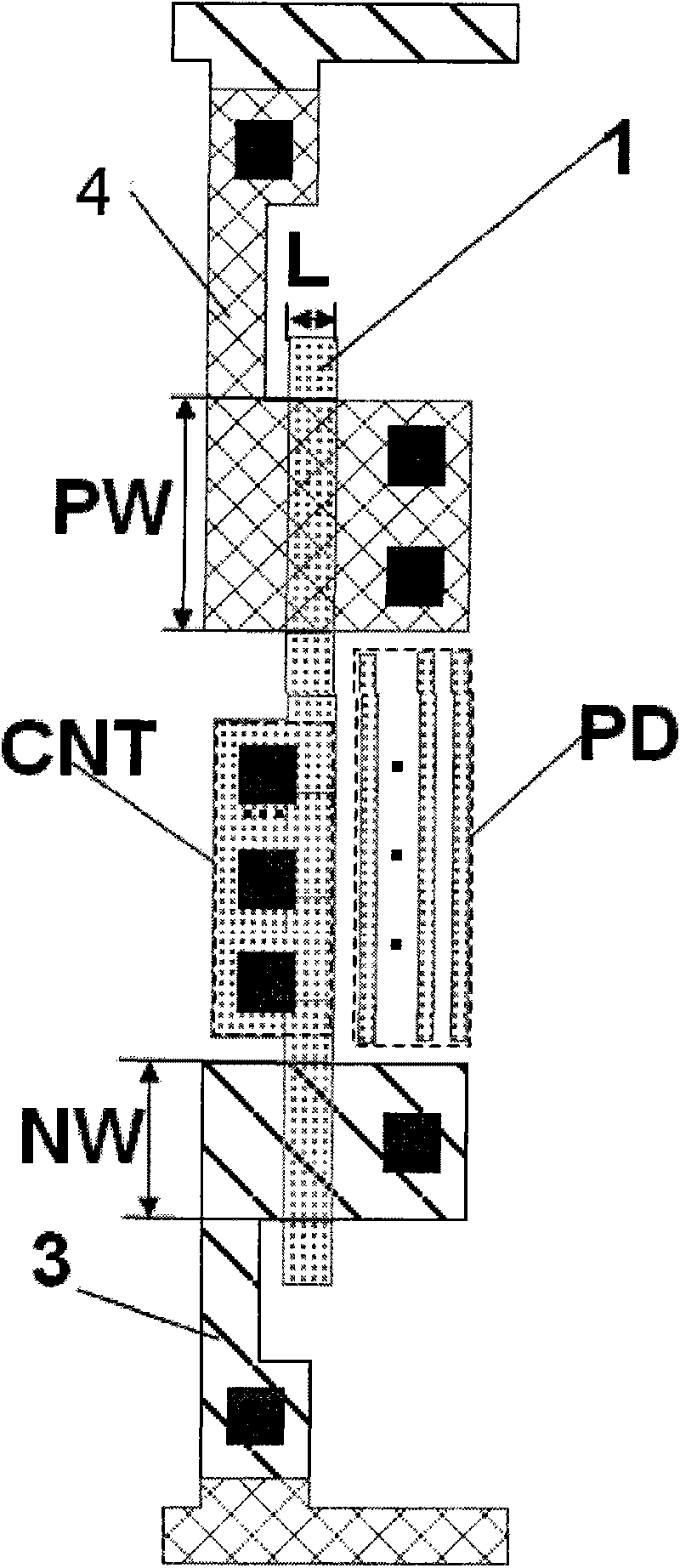
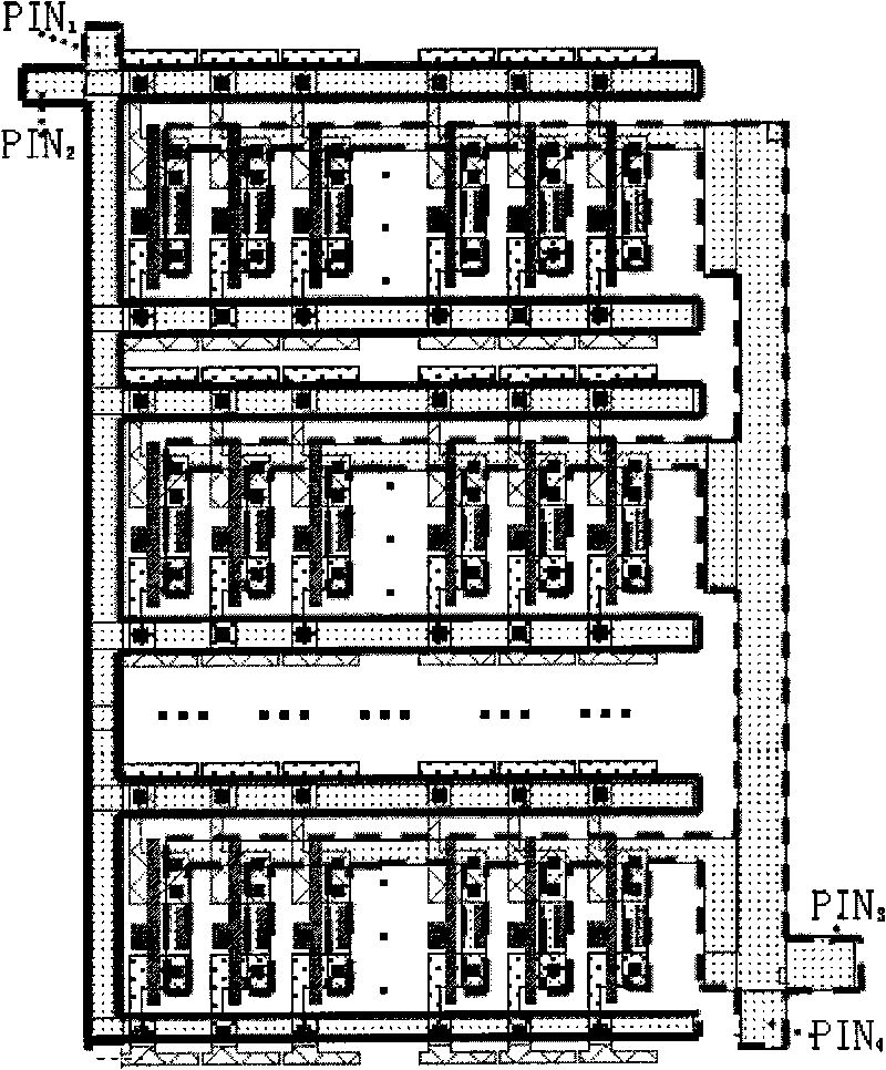
[0028] In order to make the surrounding conditions of the silicon gate of the test structure similar to the actual circuit, this method is based on the typical component transistors and typical standard cell inverters in the CMOS process, and sets the layout parameters that may affect the random defects of the silicon gate as variable parameters. , build the parameterized transistors and parameterized inverters in the array of test structures.

[0029] The CMOS process transistor has a relatively mature structure. This method parameterizes the layout structure that affects the random defects in silicon gate manufacturing. The schematic diagram of the parameterized transistor is as follows figure 1 Shown: T is the distance from the top of the silicon gate 1 to the active region 2, B is the distance from the bottom of the silicon gate 1 to the active region 2, L is the...


PUM


Abstract

The invention discloses a method for detecting random defects of a silicon gate of a CMOS process. The method comprises the following steps: designing a comb-shaped testing structure of a parametric transistor according to an orthogonal table L9 (34), and detecting leakage defects between a source electrode and a drain electrode of the transistor when the silicon gate is a control gate pole; designing a through-hole chain-type testing structure of the parametric transistor according to an orthogonal table L16 (45), and detecting broken circuit defects when the silicon gate and an upper metal are connected with each other; designing a snake-shaped testing structure of a parametric phase inverter according to an orthogonal table L16 (45), and detecting the broken circuit defects when the silicon gate is the gate pole for interconnection; and measuring an optical parameter of each testing structure by using a four electrode testing method, and analyzing the level combination of factors which remarkably affect the random defects of the silicon gate through a variance analysis method. The basic units of the testing structures are arranged by a compact mode, can effectively utilizes areas of the testing structures, and can emulate the defects of the silicon gate in an actual circuit, thereby determining the level combination of the factors which remarkably affect the optical parameters of the testing structures.

Description

technical field [0001] The invention relates to a method for detecting random defects of a silicon gate in a CMOS process, and belongs to the field of integrated circuit manufacturing. Background technique [0002] In the process of integrated circuit manufacturing, due to various uncertain reasons, there are differences between the silicon gate on the chip and the expected silicon gate in the design, which is manifested as the unexpected absence or increase of silicon material in the silicon gate, and the electrical performance is manifested as an abnormal increase in resistance or decrease. The change of silicon gate resistance will affect the performance and function of the chip, and affect the yield of the chip. [0003] These defects appear as random probabilistic events and are called stochastic defects. The causes of random defects in the silicon gate are: particles caused by machine wear, pollutants on the Wafer surface, impurities during polysilicon deposition, po...

Claims


Application Information

Patent Timeline
Patent Type & Authority Applications(China)
IPC IPC(8): H01L21/66G01R31/02
Inventor 罗小华严晓浪
Owner ZHEJIANG UNIV
Why Eureka
Try Eureka