Multilayer ceramic substrate, electronic component, and method of manufacturing multilayer ceramic substrate

一种多层陶瓷、陶瓷衬的技术,应用在多层电路制造、印刷电路制造、印刷电路零部件等方向,能够解决变窄等问题

Active Publication Date: 2010-04-07
PROTERIAL LTD
View PDF14 Cites 6 Cited by
  • Summary
  • Abstract
  • Description
  • Claims
  • Application Information

AI Technical Summary

Problems solved by technology

The interval between these electrodes is narrowed to 100 to 150 μm, and in the case of semiconductor package parts, there is a tendency to further narrow it by flip-chip mounting

Method used


Image

  • Multilayer ceramic substrate, electronic component, and method of manufacturing multilayer ceramic substrate
  • Multilayer ceramic substrate, electronic component, and method of manufacturing multilayer ceramic substrate
  • Multilayer ceramic substrate, electronic component, and method of manufacturing multilayer ceramic substrate

Examples


Embodiment Construction

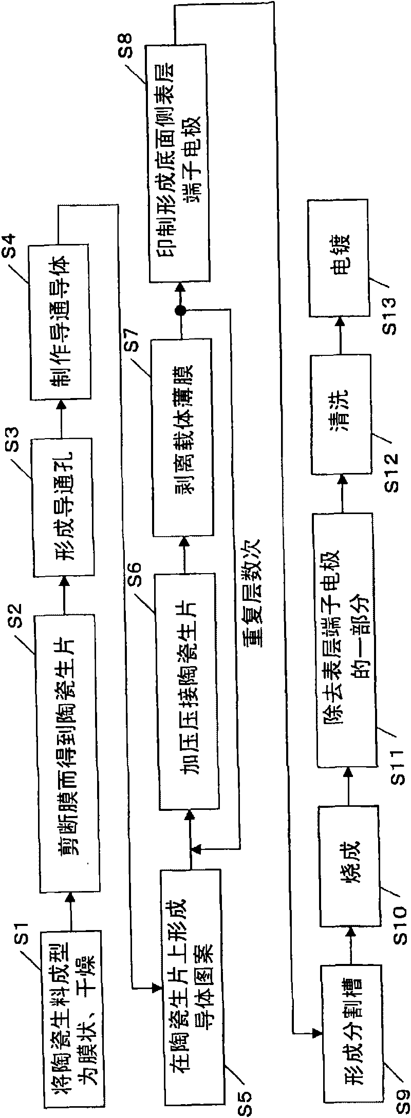
[0029] Embodiments of the present invention will be described with reference to the drawings. figure 1 It is a flowchart showing the manufacturing steps of the multilayer ceramic substrate of this embodiment.

[0030] (manufacturing of multilayer ceramic substrates)

[0031] In the step of forming the multilayer ceramic substrate of this embodiment, first, a plurality of ceramic green sheets are produced. For this reason, on the organic carrier film (carry film) (for example PET film) by doctor blade method, will be made of the ceramic material powder that can be fired at low temperature, the powder of glass component, organic binder, plasticizer and A slurry made of a mixture of solvents is formed into a film with a predetermined thickness and dried (S1). The dried thickness of the raw material varies depending on the purpose, but is about 20 to 200 μm in the example here.

[0032] In addition, as the low-temperature sinterable ceramic material used for ceramic green sheet...


PUM

PropertyMeasurementUnit
depthaaaaaaaaaa
particle diameteraaaaaaaaaa
tensile modulusaaaaaaaaaa

Abstract

A multilayer ceramic substrate in which an active element and a passive element are surface-equipped over the outermost surface on one side is provided. The multilayer ceramic substrate comprises a plurality of laminated ceramic substrate layers, a surface layer terminal electrode provided in a via hole of an outermost ceramic substrate layer on at least one side and having a surface layer via electrode and a metal plating layer deposited over an end surface of the surface layer via electrode, and a via conductor which connects the surface layer terminal electrode and circuit patterns over the ceramic substrate layer at the inside, wherein a via hole size of a surface layer terminal electrode for connection of the active element is smaller than a via hole size of a surface layer terminal electrode for connection of the passive element.

Description

technical field [0001] The invention relates to a multilayer ceramic substrate, an electronic component and a method for manufacturing the multilayer ceramic substrate. Background technique [0002] Multilayer ceramic substrates are widely used in today's increasingly high-performance and compact devices such as mobile phones. In a general multilayer ceramic substrate, a plurality of ceramic substrate layers are laminated, and a wiring layer having internal wiring is formed between the respective ceramic substrate layers. These wiring layers are connected by wirings called via wirings. [0003] A structural example of such a multilayer ceramic substrate is disclosed in JP-A-2007-305740 (Patent Document 1). The multilayer ceramic substrate disclosed in Patent Document 1 has: a ceramic laminate formed by laminating a plurality of ceramic layers; a recess formed on one main surface of the ceramic laminate; and a connection exposed inside the recess. an electrode for use; and...

Claims


Application Information

Patent Timeline
Patent Type & Authority Applications(China)
IPC IPC(8): H01L23/15H01L23/498H01L23/48H01L21/48
CPCH05K3/4629H05K3/246H05K2201/09745H05K2201/0347H05K1/0306H05K3/4061H05K3/4611H05K1/113H01L2224/16225H01L2924/15192H01L2924/19105H01L2224/05573H01L2224/05568H01L2924/00014H01L2224/05599H05K1/02H05K3/46
Inventor 池田初男市川耕司
Owner PROTERIAL LTD
Why Eureka
Try Eureka